
Owner's manual

VS-GB400TH120U
www.vishay.com
Vishay Semiconductors
Revision: 06-Mar-13
2
Document Number: 94789
For technical questions within your region: DiodesAmericas@vishay.com
, DiodesAsia@vishay.com, DiodesEurope@vishay.com
THIS DOCUMENT IS SUBJECT TO CHANGE WITHOUT NOTICE. THE PRODUCTS DESCRIBED HEREIN AND THIS DOCUMENT
ARE SUBJECT TO SPECIFIC DISCLAIMERS, SET FORTH AT www.vishay.com/doc?91000
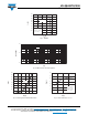
IGBT ELECTRICAL SPECIFICATIONS (T
C
= 25 °C unless otherwise noted)
PARAMETER SYMBOL TEST CONDITIONS MIN. TYP. MAX. UNITS
Collector to emitter breakdown voltage V
(BR)CES
T
J
= 25 °C 1200 - -
VCollector to emitter voltage V
CE(on)
V
GE
= 15 V, I
C
= 400 A, T
J
= 25 °C - 3.10 3.60
V
GE
= 15 V, I
C
= 400 A, T
J
= 125 °C - 3.45 -
Gate to emitter threshold voltage V
GE(th)
V
CE
= V
GE
, I
C
= 4.0 mA, T
J
= 25 °C 4.4 4.9 6.0
Collector cut-off current I
CES
V
CE
= V
CES
, V
GE
= 0 V, T
J
= 25 °C - - 5.0 mA
Gate to emitter leakage current I
GES
V
GE
= V
GES
, V
CE
= 0 V, T
J
= 25 °C - - 400 nA
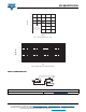
SWITCHING CHARACTERISTICS
PARAMETER SYMBOL TEST CONDITIONS MIN. TYP. MAX. UNITS
Turn-on delay time t
d(on)
V
CC
= 600 V, I
C
= 400 A, R
g
= 2.2 ,
V
GE
= ± 15 V, T
J
= 25 °C
- 680 -
ns
Rise time t
r
- 142 -
Turn-off delay time t
d(off)
- 638 -
Fall time t
f
-99-
Turn-on switching loss E
on
- 19.0 -
mJ
Turn-off switching loss E
off
- 32.5 -
Turn-on delay time t
d(on)
V
CC
= 600 V, I
C
= 400 A, R
g
= 2.2 ,
V
GE
= ± 15 V, T
J
= 125 °C
- 690 -
ns
Rise time t
r
- 146 -
Turn-off delay time t
d(off)
- 669 -
Fall time t
f
- 108 -
Turn-on switching loss E
on
- 26.1 -
mJ
Turn-off switching loss E
off
- 36.7 -
Input capacitance C
ies
V
GE
= 0 V, V
CE
= 30 V, f = 1.0 MHz
- 33.7 -
nFOutput capacitance C
oes
-2.99-
Reverse transfer capacitance C
res
-1.21-
SC data I
SC
t
p
10 μs, V
GE
= 15 V, T
J
= 25 °C,
V
CC
= 600 V, V
CEM
1200 V
- 2600 - A
Internal gate rsistance R
g
-0.5-
Stray inductance L
CE
- - 18 nH
Module lead resistance, terminal to chip R
CC’+EE’
T
C
= 25 °C - 0.32 - m
DIODE ELECTRICAL SPECIFICATIONS (T
C
= 25 °C unless otherwise noted)
PARAMETER SYMBOL TEST CONDITIONS MIN. TYP. MAX. UNITS
Forward voltage V
F
I
F
= 400 A
T
J
= 25 °C - 1.95 2.25
V
T
J
= 125 °C - 1.85 -
Reverse recovery charge Q
rr
I
F
= 400 A, V
R
= 600 V,
dI
F
/dt = - 2850 A/μs
V
GE
= - 15 V
T
J
= 25 °C - 24.1 -
μC
T
J
= 125 °C - 44.3 -
Peak reverse recovery current I
rr
T
J
= 25 °C - 220 -
A
T
J
= 125 °C - 295 -
Reverse recovery energy E
rec
T
J
= 25 °C - 13.9 -
mJ
T
J
= 125 °C - 24.8 -