
Manual

www.vishay.com For technical questions, contact: indmodules@vishay.com
Document Number: 93362
6 Revision: 31-May-11
This document is subject to change without notice.
THE PRODUCTS DESCRIBED HEREIN AND THIS DOCUMENT ARE SUBJECT TO SPECIFIC DISCLAIMERS, SET FORTH AT
www.vishay.com/doc?91000
GA300TD60S
Vishay Semiconductors
Dual INT-A-PAK Low Profile "Half-Bridge"
(Standard Speed IGBT), 300 A
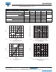
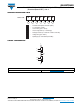
Fig. 17 - Typical Reverse Recovery Charge vs. dI
F
/dt,
V
CC
= 400 V, I
F
= 300 A
Fig. 18 - Maximum Thermal Impedance Z
thJC
Characteristics (IGBT)
Fig. 19 - Maximum Thermal Impedance Z
thJC
Characteristics (Diode)
Q
rr
(μC)
dI
F
/dt (A/μs)
100 200 400 600 800 1000300 500 700 900
0
22
16
4
2
6
8
20
12
14
18
10
93362_17
T
J
= 25 °C
T
J
= 125 °C
0.001
0.01
0.1
1
0.00001
93362_18
0.0001 0.001 0.01 0.1 1
t
1
- Rectangular Pulse Duration (s)
Z
thJC
- Thermal Impedance
Junction to Case (°C/W)
10
D = 0.50
D = 0.20
D = 0.10
D = 0.05
D = 0.02
D = 0.01
DC
0.001
0.01
0.1
1
0.00001
93362_19
0.0001 0.001 0.01 0.1 1
t
1
- Rectangular Pulse Duration (s)
Z
thJC
- Thermal Impedance
Junction to Case (°C/W)
10
D = 0.50
D = 0.20
D = 0.10
D = 0.05
D = 0.02
D = 0.01
DC