
Owner manual

VS-GA250SA60S
www.vishay.com
Vishay Semiconductors
Revision: 20-Jul-12
5
Document Number: 94704
For technical questions within your region: DiodesAmericas@vishay.com
, DiodesAsia@vishay.com, DiodesEurope@vishay.com
THIS DOCUMENT IS SUBJECT TO CHANGE WITHOUT NOTICE. THE PRODUCTS DESCRIBED HEREIN AND THIS DOCUMENT
ARE SUBJECT TO SPECIFIC DISCLAIMERS, SET FORTH AT www.vishay.com/doc?91000
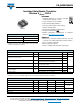
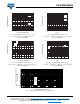
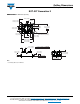
Fig. 12 - Typical Load Current vs. Frequency (Load Current = I
RMS
of Fundamental)
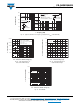
Fig. 13 - Typical Capacitance vs.
Collector to Emitter Voltage
Fig. 14 - Typical Gate Charge vs.
Gate to Emitter Voltage
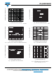
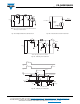
Fig. 15 - Turn-Off SOA
For both:
Duty cycle: 50 %
T
J
= 125 °C
T
sink
= 90 °C
Gate drive as specied
Power dissipation = 140 W
0
250
0.1
f - Frequency (kHz)
Load Current (A)
1 10 100
200
150
100
50
Clamp voltage:
80 % of rated
Triangular wave:
I
60 % of rated
voltage
Ideal diodes
Square wave:
I
1 10 100
0
6000
12 000
18 000
24 000
30 000
V
CE
- Collector to Emitter Voltage (V)
C - Capacitance (pF)
V
GE
= 0 V, f = 1 MHz
C
ies
= C
ge
+ C
gc
, C
ce
shorted
C
res
= C
gc
C
oes
= C
ce
+ C
gc
C
ies
C
oes
C
res
0 200 400 600 800
0
4
8
12
16
20
Q
G
- Total Gate Charge (nC)
V
GE
- Gate to Emitter Voltage (V)
V
CC
= 400 V
I
C
= 100 A
I
C
- Collector Current (A)
1
10
100
1000
1 10 100 1000
Safe operating area
V
CE
- Collector to Emitter Voltage (V)
V
GE
= 20 V
T
J
= 125 °C