6121 Baker Road, Suite 108 Minnetonka, MN 55345 Phone (952) 933-6190 Fax (952) 933-6223 1-800-274-4284 www.chtechnology.com Thank you for downloading this document from C&H Technology, Inc. Please contact the C&H Technology team for the following questions - Technical Application Assembly Availability Pricing Phone – 1-800-274-4284 E-Mail – sales@chtechnology.com www.chtechnology.com - SPECIALISTS IN POWER ELECTRONIC COMPONENTS AND ASSEMBLIES - www.chtechnology.
VS-GA250SA60S www.vishay.com Vishay Semiconductors Insulated Gate Bipolar Transistor Ultralow VCE(on), 250 A FEATURES • Standard: Optimized for minimum saturation voltage and low speed up to 5 kHz • Lowest conduction losses available • Fully isolated package (2500 VAC) • Very low internal inductance (5 nH typical) • Industry standard outline SOT-227 • Designed and qualified for industrial level • UL approved file E78996 • Material categorization: For definitions of compliance please see www.vishay.
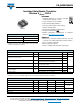
VS-GA250SA60S www.vishay.com Vishay Semiconductors ELECTRICAL SPECIFICATIONS (TJ = 25 °C unless otherwise noted) PARAMETER MIN. TYP. MAX. Collector to emitter breakdown voltage V(BR)CES VGE = 0 V, IC = 1 mA 600 - - Emitter to collector breakdown voltage V(BR)ECS (1) VGE = 0 V, IC = 1.0 A Collector to emitter voltage SYMBOL VCE(on) TEST CONDITIONS 18 - - IC = 100 A - 1.10 1.3 IC = 200 A - 1.33 1.66 IC = 100 A, TJ = 125 °C - 1.02 - - 1.32 - - 1.
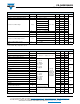
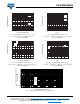
VS-GA250SA60S www.vishay.com Vishay Semiconductors 10 140 ICES - Collector Current (mA) Allowable Case Temperature (°C) 160 120 100 80 60 40 20 0 0 TJ = 150 °C 1 0.1 TJ = 125 °C 0.01 TJ = 25 °C 0.001 0.0001 100 50 100 150 200 250 300 350 400 450 500 200 300 400 500 600 VCE - Collector-to-Emitter Voltage (V) Fig.
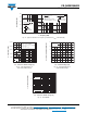
VS-GA250SA60S www.vishay.com Vishay Semiconductors 1000 Eoff Eoff 100 Energy Losses (mJ) Switching Energy (mJ) 1000 10 Eon 1 100 Eon 10 1 0.1 0.1 25 50 75 100 125 150 175 200 0 225 10 20 30 40 50 IC - Collector Current (A) Rg (Ω) Fig. 7 - Typical IGBT Energy Losses vs. IC, TJ = 125 °C, VCC = 480 V, VGE = 15 V, L = 500 μH, Rg = 5 , Diode used: 60APH06 Fig. 9 - Typical IGBT Energy Losses vs.
VS-GA250SA60S www.vishay.com Vishay Semiconductors 250 For both: Triangular wave: I Duty cycle: 50 % TJ = 125 °C Tsink = 90 °C Clamp voltage: Gate drive as specified 80 % of rated Power dissipation = 140 W Load Current (A) 200 150 Square wave: 60 % of rated voltage I 100 50 Ideal diodes 0 1 0.1 10 100 f - Frequency (kHz) Fig. 12 - Typical Load Current vs.
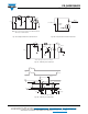
VS-GA250SA60S www.vishay.com Vishay Semiconductors L D.U.T. VC* RL = 50 V 0 V to 480 V 1000 V 480 V 4 x IC at 25 °C 480 µF 960 V 1 2 * Driver same type as D.U.T.; VC = 80 % of VCE (max) Note: Due to the 50 V power supply, pulse width and inductor will increase to obtain rated Id Fig. 16a - Clamped Inductive Load Test Circuit Fig. 16b - Pulsed Collector Current Test Circuit IC L D.U.T. Driver* VC 50 V 1000 V 1 2 3 * Driver same type as D.U.T., VC = 480 V Fig.
VS-GA250SA60S www.vishay.
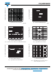
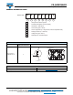
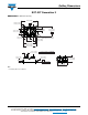
Outline Dimensions www.vishay.com Vishay Semiconductors SOT-227 Generation II DIMENSIONS in millimeters (inches) 38.30 (1.508) 37.80 (1.488) Ø 4.10 (0.161) Ø 4.30 (0.169) -A- 4 x M4 nuts 6.25 (0.246) 6.50 (0.256) 12.50 (0.492) 13.00 (0.512) 25.70 (1.012) 24.70 (0.972) -B- 7.45 (0.293) 7.60 (0.299) 14.90 (0.587) 15.20 (0.598) R full 2.10 (0.083) 2.20 (0.087) 30.50 (1.200) 29.80 (1.173) 31.50 (1.240) 32.10 (1.264) 4x 2.20 (0.087) 1.90 (0.075) 8.30 (0.327) 7.70 (0.303) 0.25 (0.
Legal Disclaimer Notice www.vishay.com Vishay Disclaimer ALL PRODUCT, PRODUCT SPECIFICATIONS AND DATA ARE SUBJECT TO CHANGE WITHOUT NOTICE TO IMPROVE RELIABILITY, FUNCTION OR DESIGN OR OTHERWISE. Vishay Intertechnology, Inc., its affiliates, agents, and employees, and all persons acting on its or their behalf (collectively, “Vishay”), disclaim any and all liability for any errors, inaccuracies or incompleteness contained in any datasheet or in any other disclosure relating to any product.