
User Manual


VS-GA200TH60S
www.vishay.com
Vishay Semiconductors
Revision: 17-Sep-12
3
Document Number: 94762
For technical questions within your region: DiodesAmericas@vishay.com
, DiodesAsia@vishay.com, DiodesEurope@vishay.com
THIS DOCUMENT IS SUBJECT TO CHANGE WITHOUT NOTICE. THE PRODUCTS DESCRIBED HEREIN AND THIS DOCUMENT
ARE SUBJECT TO SPECIFIC DISCLAIMERS, SET FORTH AT www.vishay.com/doc?91000
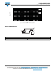
Fig. 1 - Typical Output Characteristics
Fig. 2 - Typical Transfer Characteristics
Fig. 3 - Switching Loss vs. Collector Current
Fig. 4 - Switching Loss vs. Gate Resistor
THERMAL AND MECHANICAL SPECIFICATIONS
PARAMETER SYMBOL TEST CONDITIONS MIN. TYP. MAX. UNITS
Operating junction temperature range T
J
- 40 - 150
°C
Storage temperature range T
STG
- 40 - 125
Junction to case
IGBT
R
thJC
--0.12
K/WDiode - - 0.27
Case to sink R
thCS
Conductive grease applied - 0.03 -
Mounting torque
Power terminal screw: M6 2.5 to 5.0
Nm
Mounting screw: M6 3.0 to 6.0
Weight 325 g
I
C
(A)
V
CE
(V)
0
50
100
150
200
250
300
350
400
01234
V
GE
= 15 V
25 °C
125 °C
46
8
10
0
100
150
50
200
250
300
350
400
I
C
(A)
V
GE
(V)
V
CE
= 20 V
25 °C
125 °C
0
2
4
6
8
10
12
14
16
18
20
0 100 300 400200
I
C
(A)
E
on
E
off
E
on
, E
off
(mJ)
V
GE
= ± 15 V
T
J
= 125 °C
R
g
= 4.7 Ω
V
CC
= 300 V
05 1510 20 25 30
0
20
10
5
15
25
30
R
g
(Ω)
E
on
, E
off
(mJ)
V
GE
= ± 15 V
T
J
= 125 °C
I
C
= 200 A
V
CC
= 300 V
E
on
E
off