
User Manual


VS-GA200TH60S
www.vishay.com
Vishay Semiconductors
Revision: 17-Sep-12
2
Document Number: 94762
For technical questions within your region: DiodesAmericas@vishay.com
, DiodesAsia@vishay.com, DiodesEurope@vishay.com
THIS DOCUMENT IS SUBJECT TO CHANGE WITHOUT NOTICE. THE PRODUCTS DESCRIBED HEREIN AND THIS DOCUMENT
ARE SUBJECT TO SPECIFIC DISCLAIMERS, SET FORTH AT www.vishay.com/doc?91000
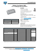
IGBT ELECTRICAL SPECIFICATIONS (T
C
= 25 °C unless otherwise noted)
PARAMETER SYMBOL TEST CONDITIONS MIN. TYP. MAX. UNITS
Collector to emitter breakdown voltage V
(BR)CES
T
J
= 25 °C 600 - -
VCollector to emitter voltage V
CE(on)
V
GE
= 15 V, I
C
= 200 A, T
J
= 25 °C - 1.9 -
V
GE
= 15 V, I
C
= 200 A, T
J
= 125 °C - 2.3 -
Gate to emitter threshold voltage V
GE(th)
V
CE
= V
GE
, I
C
= 0.25 mA, T
J
= 25 °C 3.5 4.5 5.5
Collector cut-off current I
CES
V
CE
= V
CES
, V
GE
= 0 V, T
J
= 25 °C - - 5.0 μA
Gate to emitter leakage current I
GES
V
GE
= V
GES
, V
CE
= 0 V, T
J
= 25 °C - - 400 nA
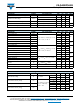
SWITCHING CHARACTERISTICS
PARAMETER SYMBOL TEST CONDITIONS MIN. TYP. MAX. UNITS
Turn-on delay time t
d(on)
V
CC
= 300 V, I
C
= 200 A, R
g
= 4.7 ,
V
GE
= ± 15 V, T
J
= 25 °C
- 106 -
ns
Rise time t
r
-45-
Turn-off delay time t
d(off)
- 460 -
Fall time t
f
-51-
Turn-on switching loss E
on
-4.2-
mJ
Turn-off switching loss E
off
-9.0-
Turn-on delay time t
d(on)
V
CC
= 300 V, I
C
= 200 A, R
g
= 4.7 ,
V
GE
= ± 15 V, T
J
= 125 °C
- 120 -
ns
Rise time t
r
-68-
Turn-off delay time t
d(off)
- 510 -
Fall time t
f
-70-
Turn-on switching loss E
on
-5.1-
mJ
Turn-off switching loss E
off
- 11.3 -
Input capacitance C
ies
V
GE
= 0 V, V
CE
= 25 V, f = 1.0 MHz
- 13.1 -
nFOutput capacitance C
oes
-0.71-
Reverse transfer capacitance C
res
-0.38-
SC data I
SC
t
sc
10 μs, V
GE
= 15 V, T
J
= 125 °C,
V
CC
= 300 V, V
CEM
600 V
- 650 - A
Stray inductance L
CE
- - 20 nH
Module lead resistance, terminal to chip R
CC’+EE’
T
C
= 25 °C - 0.35 - m
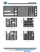
DIODE ELECTRICAL SPECIFICATIONS (T
C
= 25 °C unless otherwise noted)
PARAMETER SYMBOL TEST CONDITIONS MIN. TYP. MAX. UNITS
Diode forward voltage V
F
I
F
= 200 A
T
J
= 25 °C - 1.4 1.6
V
T
J
= 125 °C - 1.6 1.8
Diode reverse recovery charge Q
rr
I
F
= 200 A, V
R
= 300 V,
dI/dt = - 6000 A/μs,
V
GE
= - 15 V
T
J
= 25 °C - 9 -
μC
T
J
= 125 °C - 16 -
Diode peak reverse recovery current I
rr
T
J
= 25 °C - 140 -
A
T
J
= 125 °C - 165 -
Diode reverse recovery energy E
rec
T
J
= 25 °C - 2.4 -
mJ
T
J
= 125 °C - 4.2 -