6121 Baker Road, Suite 108 Minnetonka, MN 55345 Phone (952) 933-6190 Fax (952) 933-6223 1-800-274-4284 www.chtechnology.com Thank you for downloading this document from C&H Technology, Inc. Please contact the C&H Technology team for the following questions - Technical Application Assembly Availability Pricing Phone – 1-800-274-4284 E-Mail – sales@chtechnology.com www.chtechnology.com - SPECIALISTS IN POWER ELECTRONIC COMPONENTS AND ASSEMBLIES - www.chtechnology.
VS-EMG050J60N www.vishay.com Vishay Semiconductors Dual Mode PFC, 60 A FEATURES • • • • • • • • • EMIPAK2 NPT Warp2 PFC IGBT with low VCE(ON) Silicon carbide PFC diode Antiparallel FRED Pt® fast recovery Integrated thermistor Square RBSOA Operating frequency 60 kHz to 150 kHz Low internal inductances Low switching loss Compliant to RoHS Directive 2002/95/EC DESCRIPTION VS-EMG050J60N is an integrated solution for dual stage PFC converter in a single package.
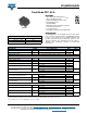
VS-EMG050J60N www.vishay.com Vishay Semiconductors ELECTRICAL SPECIFICATIONS (TJ = 25 °C unless otherwise noted) PARAMETER SYMBOL TEST CONDITIONS MIN. TYP. MAX. UNITS PFC IGBT Q1 - Q2 Collector to emitter breakdown voltage Temperature coefficient of breakdown voltage BVCES VGE = 0 V, IC = 500 μA 600 - - V BVCES/TJ VGE = 0 V, IC = 500 μA (25 °C to 125 °C) - 0.1 - V/°C VGE = 15 V, IC = 27 A - 1.44 1.75 VGE = 15 V, IC = 50 A - 1.8 2.1 VGE = 15 V, IC = 27 A, TJ = 125 °C - 1.
VS-EMG050J60N www.vishay.com Vishay Semiconductors SWITCHING CHARACTERISTICS (TJ = 25 °C unless otherwise noted) PARAMETER SYMBOL Turn-on switching loss EON Turn-off switching loss EOFF Total switching loss ETOT Turn-on delay time td(on) Rise time Turn-off delay time Fall time TEST CONDITIONS tr td(off) MIN. TYP. MAX. - 0.182 - IC = 50 A VCC = 400 V VGE = 15 V Rg = 4.7 L = 500 μH TJ = 125 °C (1) - 0.615 - - 0.
VS-EMG050J60N www.vishay.com Vishay Semiconductors THERMAL AND MECHANICAL SPECIFICATIONS PARAMETER SYMBOL MIN. - - 0.37 RthJC - - 4.29 Q1 - Q2 PFC IGBT - Junction to case thermal resistance (per switch) D1 - D2 AP diode - Junction to case thermal resistance (per diode) TYP. MAX. D3 - D4 PFC diode - Junction to case thermal resistance (per diode) - - 1.69 Q1 - Q2 PFC IGBT - Case to sink thermal resistance (per switch) - 0.
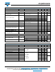
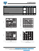
VS-EMG050J60N www.vishay.com Vishay Semiconductors 100 1 VCE = 20 V 90 80 0.1 125 °C ICES (mA) 70 ICE (A) 60 TJ = 125 °C 50 40 TJ = 25 °C 0.01 25 °C 30 0.001 20 10 0 3 4 5 6 7 VGE (V) 93495_05 0.0001 100 8 200 300 400 500 600 VCES (V) 93495_08 Fig. 8 - Typical PFC IGBT Zero Gate Voltage Collector Current Fig. 5 - Typical PFC IGBT Transfer Characteristics 4.5 100 90 TJ = 25 °C 80 4.0 60 IF (A) Vgeth (V) 70 3.5 50 40 3.0 TJ = 125 °C 30 TJ = 125 °C TJ = 25 °C 20 2.
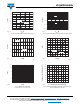
VS-EMG050J60N www.vishay.com Vishay Semiconductors 50 1.8 1.6 40 1.4 Energy (mJ) TJ = 25 °C IF (A) 30 TJ = 125 °C 20 1.2 1.0 Eoff 0.8 0.6 0.4 10 Eon 0.2 0 0 0 0.5 1.0 1.5 2.0 2.5 3.0 3.5 4.0 VFM (V) 93495_11 0 40 60 80 100 IC (A) Fig. 14 - Typical PFC IGBT Energy Loss vs. IC (with Freewheeling D3 - D4 PFC Diode) TJ = 125 °C, VCC = 400 V, Rg = 4.7 , VGE = 15 V, L = 500 μH 1000 160 140 Switching Time (ns) Allowable Case Temperature (°C) Fig.
VS-EMG050J60N www.vishay.com Vishay Semiconductors 17 70 15 60 13 50 125 °C 125 °C trr (ns) Irr (A) 11 9 40 25 °C 30 7 20 5 3 100 200 300 400 10 100 500 dIF/dt (A/μs) 93495_17 200 300 400 500 dIF/dt (A/μs) 93495_19 Fig. 19 - Typical PFC Diode Reverse Recovery Time vs. dIF/dt VR = 200 V, IF = 10 A Fig. 17 - Typical Antiparallel Reverse Recovery Current vs. dIF/dt VR = 200 V, IF = 20 A 600 4.5 550 3.5 125 °C 450 Irr (A) Qrr (nC) 500 400 125 °C 2.5 350 300 1.
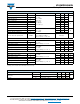
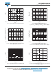
VS-EMG050J60N www.vishay.com Vishay Semiconductors ZthJC - Thermal Impedance Junction to Case (°C/W) 1 0.1 D = 0.50 D = 0.20 D = 0.10 D = 0.05 D = 0.02 D = 0.01 DC 0.01 0.001 0.00001 0.0001 0.001 0.01 0.1 1 10 1 10 t1 - Rectangular Pulse Duration (s) 93495_22 Fig. 22 - Maximum Thermal Impedance ZthJC Characteristics (IGBT) ZthJC - Thermal Impedance Junction to Case (°C/W) 10 1 D = 0.50 D = 0.20 D = 0.10 D = 0.05 D = 0.02 D = 0.01 DC 0.1 0.01 0.00001 0.0001 0.001 0.01 0.
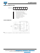
VS-EMG050J60N www.vishay.com Vishay Semiconductors ORDERING INFORMATION TABLE Device code VS- EM G 050 J 60 N 1 2 3 4 5 6 7 1 - Vishay Semiconductors product 2 - Package indicator (EM = EMIPAK2) 3 - Circuit configuration (G = Dual mode PFC) 4 - Current rating (050 = 50 A) 5 - Die technology (J = Warp2 IGBT) 6 - Voltage rating (60 = 600 V) 7 - N = Ultrafast TYPICAL CONNECTION Note • Please refer to lead assignment for correct pin configuration.
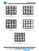
VS-EMG050J60N www.vishay.com Vishay Semiconductors CIRCUIT CONFIGURATION D3 11 17 33 35 Q1 D1 6 5 13 24 14 Th 15 23 Q2 D2 2 1 D4 27 30 28 36 PACKAGE 6 2 5 1 13 14 15 11 33 36 30 24 23 17 28 35 27 LINKS TO RELATED DOCUMENTS Dimensions Revision: 09-Dec-11 www.vishay.com/doc?95436 Document Number: 93495 10 For technical questions within your region: DiodesAmericas@vishay.com, DiodesAsia@vishay.com, DiodesEurope@vishay.com THIS DOCUMENT IS SUBJECT TO CHANGE WITHOUT NOTICE.
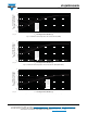
Outline Dimensions Vishay Semiconductors EMIPAK2 DIMENSIONS in millimeters 15.2 12.7 8.9 Front view 55 ± 0.3 Pins position with tolerance Ø 1 ± 0.1 M4 Ø 0.4 5.1 14 11.4 10.2 7.6 7.6 6.4 3.8 2.6 1.3 13.3 3.2 1.9 1.3 5.1 2.5 6.3 Detail “A” Scale 10:1 Detail “A” 5° F 14 F 7 15.9 12.1 8.3 5.7 39 ± 0.3 5 62 ± 0.3 41.5 23 53 62 ± 0.3 Ø2 Ø 12.1 20.5 ± 1 3 ref. Top view 9.5 9.5 15.9 10.8 Side view 7 Ø 4.3 5.7 1.9 12 20.5 ± 1 17 ± 1 3.8 16.8 8.9 10.1 12.7 11.4 16.5 16.5 20.
Legal Disclaimer Notice www.vishay.com Vishay Disclaimer ALL PRODUCT, PRODUCT SPECIFICATIONS AND DATA ARE SUBJECT TO CHANGE WITHOUT NOTICE TO IMPROVE RELIABILITY, FUNCTION OR DESIGN OR OTHERWISE. Vishay Intertechnology, Inc., its affiliates, agents, and employees, and all persons acting on its or their behalf (collectively, “Vishay”), disclaim any and all liability for any errors, inaccuracies or incompleteness contained in any datasheet or in any other disclosure relating to any product.