
User Manual


VS-40MT1.0P.PbF, VS-70MT1.0P.PbF, VS-100MT1.0P.PbF Series
www.vishay.com
Vishay Semiconductors
Revision: 30-Oct-13
4
Document Number: 94538
For technical questions within your region: DiodesAmericas@vishay.com
, DiodesAsia@vishay.com, DiodesEurope@vishay.com
THIS DOCUMENT IS SUBJECT TO CHANGE WITHOUT NOTICE. THE PRODUCTS DESCRIBED HEREIN AND THIS DOCUMENT
ARE SUBJECT TO SPECIFIC DISCLAIMERS, SET FORTH AT www.vishay.com/doc?91000
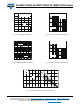
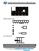
Fig. 6 - Current Rating Characteristics
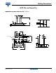
Fig. 7 - On-State Voltage Drop Characteristics
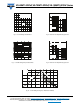
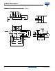
Fig. 8 - Maximum Non-Repetitive Surge Current
Fig. 9 - Maximum Non-Repetitive Surge Current
Fig. 10 - Current Rating Nomogram (1 Module Per Heatsink)
Total Output Current (A)
Maximum Allowable Case Temperature (°C)
60
70
80
90
100
110
120
130
140
150
160
0 1020304050607080
120˚
(Rect)
70MT...P
R (DC) = 0.23 K/W
Per Module
thJC
Instantaneous On-state Current (A)
Instantaneous On-state Voltage (V)
1
10
100
1000
012345
Tj = 150˚C
Tj = 25˚C
70MT...P
Number Of Equal Amplitude Half Cycle Current Pulses (N)
Peak Half Sine Wave On-state Current (A)
100
150
200
250
300
350
110100
At Any Rated Load Condition And With
Rated Vrrm Applied Following Surge.
Initial Tj = 150˚C
@ 60 Hz 0.0083 s
@ 50 Hz 0.0100 s
70MT...P
Per Junction
Pulse Train Duration(s)
Peak Half Sine Wave On-state Current (A)
50
100
150
200
250
300
350
400
0.01 0.1 1
Maximum Non Repetitive Surge Current
Versus Pulse Train Duration. Control
Of Conduction May Not Be Maintained.
Initial T j = 150˚C
No Voltage Reapplied
Rated V rrm Reapplied
70MT...P
Per Junction
Maximum Allowable Ambient Temperature (°C)
Total Output Current (A)
Maximum Total Power Loss (W)
0306090120150
RthSA = 0.1 K/W - Delta R
0.3 K/W
0.4 K/W
0.5 K/W
1 K/W
0.2 K/W
0
50
100
150
200
250
300
020406080
120˚
(Rect)
Tj = 150˚C
70MT...P