6121 Baker Road, Suite 108 Minnetonka, MN 55345 Phone (952) 933-6190 Fax (952) 933-6223 (800) 274-4284 Thank you for downloading this document from C&H Technology, Inc. Please contact the C&H Technology team for the following questions - Technical Application Assembly Availability Pricing Phone – 1-800-274-4284 E-Mail – sales@chtechnology.com C & H TECHNOLOGY, INC. ● 6121 BAKER RD. SUITE 108 ● MINNETONKA, MINNESOTA 55345 ● 800-274-4284 ● 952-933-6190 ● FAX: 952-933-6223 ● WWW.CHTECHNOLOGY.
VS-40MT1.0P.PbF, VS-70MT1.0P.PbF, VS-100MT1.0P.PbF Series www.vishay.com Vishay Semiconductors Three Phase Bridge (Power Modules), 45 A to 100 A FEATURES • • • • • • • • • MT...PA MT...
VS-40MT1.0P.PbF, VS-70MT1.0P.PbF, VS-100MT1.0P.PbF Series www.vishay.com Vishay Semiconductors FORWARD CONDUCTION PARAMETER Maximum DC output current at case temperature SYMBOL IO TEST CONDITIONS 120° rect. to conduction angle t = 10 ms Maximum peak, one cycle forward, non-repetitive on state surge current IFSM No voltage reapplied t = 8.3 ms t = 10 ms 100 % VRRM reapplied t = 8.3 ms t = 10 ms Maximum I2t for fusing I 2t No voltage reapplied t = 8.
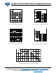
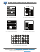
VS-40MT1.0P.PbF, VS-70MT1.0P.PbF, VS-100MT1.0P.PbF Series 160 Vishay Semiconductors 40MT...P R thJC (DC) = 0.27 K/W Per Module 150 140 130 120 120˚ (Rect) 110 100 90 80 0 10 20 30 40 250 Peak Half Sine Wave On-state Current (A) Maximum Allowable Case Temperature (°C) www.vishay.com 200 150 100 40MT...P Per Junction 50 50 1 Fig. 1 - Current Rating Characteristics Tj = 150˚C 10 40MT...
VS-40MT1.0P.PbF, VS-70MT1.0P.PbF, VS-100MT1.0P.PbF Series Vishay Semiconductors 160 Peak Half Sine Wave On-state Current (A) Maximum Allowable Case Temperature (°C) www.vishay.com 70MT...P R thJC (DC) = 0.23 K/W Per Module 150 140 130 120 110 120˚ (Rect) 100 90 80 70 60 0 250 200 150 100 1 Tj = 150˚C 100 10 70MT...P 1 3 400 Peak Half Sine Wave On-state Current (A) Tj = 25˚C 2 10 100 Fig. 8 - Maximum Non-Repetitive Surge Current 1000 1 70MT...
VS-40MT1.0P.PbF, VS-70MT1.0P.PbF, VS-100MT1.0P.PbF Series Vishay Semiconductors 140 Peak Half Sine Wave On-state Current (A) Maximum Allowable Case Temperature (°C) www.vishay.com 100MT...P R thJC (DC) = 0.19 K/W 120 Per Module 100 80 120˚ (Rect) 60 40 40 50 60 70 80 90 100 110 120 130 Peak Half Sine Wave On-state Current (A) Instantaneous On-state Current (A) 100MT...P 100 10 Tj = 150˚C Tj = 25˚C 2 2.5 3 300 250 200 100MT...P Per Junction 150 100 10 100 Fig.
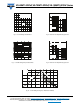
VS-40MT1.0P.PbF, VS-70MT1.0P.PbF, VS-100MT1.0P.PbF Series Transient Thermal Impedance Z thJC (K/W) www.vishay.com Vishay Semiconductors 10 Steady State Value RthJC per junction = 1.6 K/W (40MT...P) 1 1.38 K/W (70MT...P 1.14 K/W (100MT...P) 40MT...P 70MT...P 100MT...P DC Operation) 0.1 0.01 0.0001 0.001 0.01 0.1 Square Wave Pulse Duration (s) 1 10 Fig.
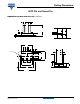
Outline Dimensions Vishay Semiconductors MTP Flat and Round Pin DIMENSIONS FOR MTP WITH FLAT PIN in millimeters 14 7 Electrical circuit 2 42 ± 0.1 3, 4 4 5 6 7 12 2.5 1, 2 44.5 7 7 7 7.4 7 22 Ø 5.2 (x 2) 22 1 6 5 7 14 14 39.5 1.3 27.5 2 3 32.5 ± 0.5 0.5 4 0.5 5.5 5.5 Ø5 16 10.5 12 ± 0.5 48.7 63.5 ± 0.25 Document Number: 95244 Revision: 07-Nov-07 For technical questions, contact: indmodules@vishay.com www.vishay.
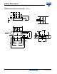
Outline Dimensions MTP Flat and Round Pin Vishay Semiconductors DIMENSIONS FOR MTP WITH ROUND PIN in millimeters 14 Ø5 7 4 Electrical circuit 7 20.5 ± 0.1 3, 4 12 2.5 5 6 7 1, 2 44.5 7 7 7 Ø 1.1 7 5 6 14 4 10.5 1 32.5 ± 0.1 2 27.5 3 22 4 12 ± 0.5 Ø5 Ø 5.2 (x 2) 16 7 14 7.4 31.8 1.3 39.5 48.7 63.5 ± 0.25 www.vishay.com 2 For technical questions, contact: indmodules@vishay.
Legal Disclaimer Notice www.vishay.com Vishay Disclaimer ALL PRODUCT, PRODUCT SPECIFICATIONS AND DATA ARE SUBJECT TO CHANGE WITHOUT NOTICE TO IMPROVE RELIABILITY, FUNCTION OR DESIGN OR OTHERWISE. Vishay Intertechnology, Inc., its affiliates, agents, and employees, and all persons acting on its or their behalf (collectively, “Vishay”), disclaim any and all liability for any errors, inaccuracies or incompleteness contained in any datasheet or in any other disclosure relating to any product.