6121 Baker Road, Suite 108 Minnetonka, MN 55345 Phone (952) 933-6190 Fax (952) 933-6223 1-800-274-4284 www.chtechnology.com Thank you for downloading this document from C&H Technology, Inc. Please contact the C&H Technology team for the following questions - Technical Application Assembly Availability Pricing Phone – 1-800-274-4284 E-Mail – sales@chtechnology.com www.chtechnology.com - SPECIALISTS IN POWER ELECTRONIC COMPONENTS AND ASSEMBLIES - www.chtechnology.
VS-100MT060WDF www.vishay.
VS-100MT060WDF www.vishay.
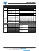
VS-100MT060WDF www.vishay.com Vishay Semiconductors SWITCHING CHARACTERISTICS (TJ = 25 °C unless otherwise noted) PARAMETER SYMBOL MIN. TYP. MAX. - 460 - - 160 - - 70 - Eon - 0.2 - Turn-off switching loss Eoff - 0.96 - Total switching loss Etot - 1.
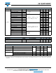
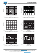
VS-100MT060WDF www.vishay.com Vishay Semiconductors 160 250 200 120 VGE = 18 V 100 IC (A) Maximum Allowable Case Temperature (°C) 140 80 150 VGE = 15 V VGE = 9 V 100 60 VGE = 12 V 40 50 20 0 0 20 40 60 80 100 120 IC - Continuous Collector Current (A) 93412_01 0 140 0 2 3 4 5 VCE (V) Fig. 4 - Typical IGBT Output Characteristics, TJ = 125 °C Fig. 1 - Maximum IGBT Continuous Collector Current vs.
VS-100MT060WDF www.vishay.com Vishay Semiconductors TJ = 25 °C 4.5 Vgeth (V) IF - Instantaneous Forward Drop (A) 5.0 4.0 3.5 TJ = 125 °C 3.0 0.2 0.3 0.4 0.5 0.6 0.7 0.8 0.9 90 70 60 40 20 10 0 0.25 80 70 60 50 TJ = 150 °C TJ = 125 °C 20 TJ = 25 °C 1.25 1.75 2.25 2.75 3.25 3.75 VF - Forward Voltage Drop (V) 160 140 120 100 80 60 40 20 0 0 0.5 1.0 1.5 2.0 2.5 0 3.0 VF - Anode to Cathode Forward Voltage Drop (V) Fig.
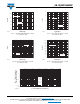
VS-100MT060WDF www.vishay.com Vishay Semiconductors 1000 2.0 td(off) Switching Time (ns) Energy (mJ) 1.6 1.2 Eoff 0.8 td(on) 100 tf tr Eon 0.4 0 10 0 20 40 60 80 100 120 IC (A) 93412_13 0 10 20 30 40 50 Rg (Ω) 93412_16 Fig. 16 - Typical IGBT Switching Time vs. Rg, TJ = 125 °C IC = 100 A, VCE = 360 V, VGE = 15 V, L = 500 μH Fig. 13 - Typical IGBT Energy Loss vs.
VS-100MT060WDF www.vishay.com Vishay Semiconductors 20 1500 TJ = 125 °C 15 TJ = 125 °C Irr (A) Qrr (nC) 1200 900 10 TJ = 25 °C 5 600 300 100 200 300 400 0 100 500 dIF/dt (A/μs) 93412_19 TJ = 25 °C 200 300 400 500 dIF/dt (A/μs) 93412_21 Fig. 21 - Typical Irr Chopper Diode vs. dIF/dt Vrr = 200 V, IF = 60 A Fig. 19 - Typical Qrr Antiparallel Diode vs.
VS-100MT060WDF www.vishay.com Vishay Semiconductors ZthJC - Thermal Impedance Junction to Case (°C/W) 10 1 D = 0.50 D = 0.20 D = 0.10 D = 0.05 D = 0.02 D = 0.01 DC 0.1 0.01 0.0001 0.001 0.01 0.1 1 10 t1 - Rectangular Pulse Duration (s) 93412_24 Fig. 24 - Maximum Thermal Impedance ZthJC Characteristics (PFC Diode) Driver L D.U.T. 0 + VCC - D + C - 1K 900 V D.U.T. Fig. C.T.1 - Gate Charge Circuit (Turn-Off) Fig. C.T.3 - S.C. SOA Circuit L Diode clamp/ D.U.T. + - 80 V L + - -5V D.
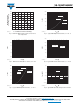
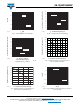
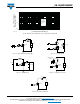
VS-100MT060WDF www.vishay.com Vishay Semiconductors CIRCUIT CONFIGURATION E1 F1 Q1 D1 D3 A7 E6 M2 M3 A1 B1 E7 Th Q4 G6 D4 D2 G7 M7 I1 L1 DIMENSIONS in millimeters 12.1 ± 0.3 Ø 1.1 ± 0.025 2.1 1.5 3.0 39.5 ± 0.3 12 ± 0.3 17± 0.3 3 2.5 ± 0.1 6 z detail Use Self Tapping Screw or M2.5 x X. e.g. M2.5 x 6 or M2.5 x 8 according to Pcb thickness used 45 ± 0.1 63.5 ± 0.15 0.8 Ra 48.7 ± 0.3 1.3 21.1 ± 0.5 7.4 4.1 A B C D E F G H I L M X 7 6 Ø 2.1(X4) 12 27.5 ± 0.3 Diam.
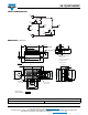
Outline Dimensions Vishay Semiconductors MTP - Full Pin DIMENSIONS in millimeters 3.0 2.1 1.5 z detail 12 ± 0.3 39.5 ± 0.3 6 12 ± 0.3 Ø 1.1 ± 0.025 3 Use self taping screw or M2.5 x X. e.g. M2.5 x 6 or M2.5 x 8 according to PCB thickness used 17 ± 0.3 2.5 ± 0.1 45 ± 0.1 63.5 ± 0.15 0.8 Ra 1.3 21.1 7.4 48.7 ± 0.3 Ø 1 ± 0.025 + 0.5 - 0.2 4.1 A B C D E F G H I L M 1 45° 19.8 ± 0.1 2 27.5 ± 0.3 31.8 ± 0.15 3 7.6 4 15.2 5 22.8 Ø 5 (x 4) 33.2 ± 0.3 6 7 5.2 Ø 2.1 (x 4) R2.
Legal Disclaimer Notice www.vishay.com Vishay Disclaimer ALL PRODUCT, PRODUCT SPECIFICATIONS AND DATA ARE SUBJECT TO CHANGE WITHOUT NOTICE TO IMPROVE RELIABILITY, FUNCTION OR DESIGN OR OTHERWISE. Vishay Intertechnology, Inc., its affiliates, agents, and employees, and all persons acting on its or their behalf (collectively, “Vishay”), disclaim any and all liability for any errors, inaccuracies or incompleteness contained in any datasheet or in any other disclosure relating to any product.