6121 Baker Road, Suite 108 Minnetonka, MN 55345 Phone (952) 933-6190 Fax (952) 933-6223 1-800-274-4284 www.chtechnology.com Thank you for downloading this document from C&H Technology, Inc. Please contact the C&H Technology team for the following questions - Technical Application Assembly Availability Pricing Phone – 1-800-274-4284 E-Mail – sales@chtechnology.com www.chtechnology.com - SPECIALISTS IN POWER ELECTRONIC COMPONENTS AND ASSEMBLIES - www.chtechnology.
Bulletin I25187 rev. B 04/00 ST333C..
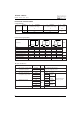
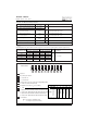
ST333C..L Series Bulletin I25187 rev. B 04/00 ELECTRICAL SPECIFICATIONS Voltage Ratings Voltage VDRM /VRRM , maximum VRSM , maximum I DRM/I RRM max. Code repetitive peak voltage non-repetitive peak voltage @ TJ = TJ max. V V mA 04 400 500 08 800 900 Type number ST333C..
ST333C..L Series Bulletin I25187 rev. B 04/00 On-state Conduction Parameter V TM Max. peak on-state voltage V T(TO)1 Low level value of threshold voltage V T(TO)2 High level value of threshold voltage r t1 Low level value of forward slope resistance ST333C..L Units 1.96 0.91 ITM= 1810A, T J = TJ max, tp = 10ms sine wave pulse V 0.58 mΩ IH 600 IL Typical latching current 1000 (16.7% x π x IT(AV) < I < π x IT(AV)), TJ = TJ max. (I > π x IT(AV)), TJ = TJ max. 0.
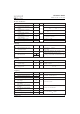
ST333C..L Series Bulletin I25187 rev. B 04/00 Thermal and Mechanical Specification Parameter ST333C..L TJ Max. operating temperature range -40 to 125 T Max. storage temperature range -40 to 150 stg RthJ-hs Max. thermal resistance, 0.011 case to heatsink K/W 0.005 Mounting force, ± 10% wt DC operation single side cooled K/W 0.05 RthC-hs Max. thermal resistance, Approximate weight Case style Conditions °C 0.
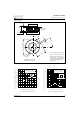
ST333C..L Series Bulletin I25187 rev. B 04/00 Outline Table 34 (1.34) DIA. MAX. 0.7 (0.03) MIN. 2 7 (1 . 0 6 ) M A X . TWO PLACES PIN RECEPTACLE AMP. 60598-1 53 (2.09) DIA. MAX. 0.7 (0.03) MIN. 6.2 (0.24) MIN. 20°± 5° 5 8 .5 (2 .3 ) D I A . M AX . 4.7 (0.18) Case Style TO-200AC (B-PUK) 36.5 (1.44) All dimensions in millimeters (inches) 2 HOLES DIA. 3.5 (0.14) x 2.5 (0.
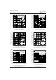
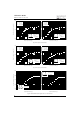
ST333C..L Series 13 0 ST 3 3 3 C ..L Se rie s (D o ub le S id e C o o le d ) R thJ- hs (D C ) = 0 .0 5 K /W 12 0 11 0 10 0 90 80 Co nd uctio n A ng le 70 60 3 0° 50 60° 40 90° 1 20° 180 ° 30 20 0 1 00 20 0 3 0 0 4 0 0 5 00 6 0 0 70 0 8 00 M a x im u m A llo w a b le H e a tsin k T e m p e ra t ure (° C ) M a x im u m A llo w a b le H e a tsin k T e m p e rat u re (°C ) Bulletin I25187 rev. B 04/00 130 ST 3 3 3 C ..L S e rie s (D o u b le Sid e C o o le d ) R th J-hs (D C ) = 0 .
ST333C..L Series Bulletin I25187 rev. B 04/00 T ra n sie n t T h e rm a l Im p e d a n c e Z th J- hs (K / W ) Instanta neous On-state Current (A) 10000 1000 T J = 25°C T J = 125°C ST333C..L Series 100 0 1 2 3 4 5 6 7 1 St e a d y St a t e V a lu e R thJ-hs = 0 .1 1 K / W (Sin g le Sid e C o o le d ) R th J- hs = 0 .0 5 K / W 0 .1 (D o ub le Sid e C o o le d ) (D C O p e ra tio n ) 0 .0 1 S T 3 3 3 C ..L Se rie s 0 .0 0 1 0 .0 0 1 0.
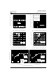
ST333C..L Series Bulletin I25187 rev. B 04/00 P e a k O n -st a t e C urre n t ( A ) 1E4 Snub ber c irc uit R s = 10 o hm s C s = 0 .47 µF V D = 80 % V D RM Snub ber circuit R s = 10 o hm s C s = 0.4 7 µF V D = 80% V D RM 1 000 40 0 5 00 20 0 100 50 Hz 100 0 15 00 1E3 1 00 50 Hz 1 50 0 20 00 20 00 25 00 25 00 3 00 0 5 000 1E2 1E1 40 0 20 0 5 00 ST3 33C ..L Se ries Trape zoidal pulse T C = 40°C d i/dt = 5 0A /µs tp 1 E2 5 00 0 tp 1 E14E 41 E1 1E 1 1 E3 ST33 3C ..
ST333C..L Series Bulletin I25187 rev. B 04/00 10 Rectangular gate pulse a) Recommended load line for rated di/dt : 20V, 10ohms; tr<=1 µs b) Recommended load line for <=30% rated di/dt : 10V, 10ohms tr<=1 µs (1) PGM = 10W, (2) PGM = 20W, (3) PGM = 40W, (4) PGM = 60W, tp = 20ms tp = 10ms tp = 5ms tp = 3.3ms (a) (b) Tj=25 °C 1 Tj=-40 °C Tj=125 °C Instantaneous Gate Voltage (V) 100 (1) (2) (3) (4) VGD IGD 0.1 0.001 0.01 Device: ST333C..L Series Frequency Limited by PG(AV) 0.