6121 Baker Road, Suite 108 Minnetonka, MN 55345 Phone (952) 933-6190 Fax (952) 933-6223 1-800-274-4284 www.chtechnology.com Thank you for downloading this document from C&H Technology, Inc. Please contact the C&H Technology team for the following questions - Technical Application Assembly Availability Pricing Phone – 1-800-274-4284 E-Mail – sales@chtechnology.com www.chtechnology.com - SPECIALISTS IN POWER ELECTRONIC COMPONENTS AND ASSEMBLIES - www.chtechnology.
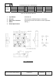
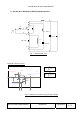
SECURITY CODE Spec. NAME Customer’s Std. Spec. Prepared by Checked by Approved by DATE MITSUBISHI ELECTRIC CORPORATION K.Kurachi R E H.Yamaguchi V 10-Apr.-2008 HIGH VOLTAGE DIODE MODULE 1. Type Number RM900DB-90S 2. Structure Flat base type (Insulated package, Cu base plate) 3. Application & Customer High power converters & Inverters for traction application 4. Outline See Fig. 1 5. Related Specifications Fig.
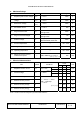
MITSUBISHI ELECTRIC CORPORATION 6. Maximum Ratings Item Symbol Conditions Ratings Unit 6.1 Repetitive peak reverse voltage VRRM Tj = 25 °C 4500 V 6.2 Non-repetitive peak reverse voltage VRSM Tj = 25 °C 4500 V 6.3 Reverse DC voltage VR(DC) Tj = 25 °C 3000 V 6.4 DC forward current IF Tc = 25 °C 900 A 6.5 Surge forward current IFSM Tj = 25 °C start, tw = 8.3 ms Half sign wave 6400 A 6.6 Surge current load integral I2t Tj = 25 °C start, tw = 8.
MITSUBISHI ELECTRIC CORPORATION 8. Thermal Characteristics Item 8.1 Symbol Thermal resistance Limits Conditions Junction to case (per 1/2 module) Rth(j-c)R Unit Min. Typ. Max. — — 20.0 K/kW — 16.0 — K/kW (Note 2) 8.2 Contact thermal resistance Case to fin Conductive grease applied (per 1/2 module) Rth(c-f) Note 2: Thermal conductivity is 1W/mK with a thickness of 100µm. 9. Mechanical Characteristics Item Symbol Conditions Limits Min. Typ. Max. Unit 9.
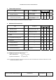
MITSUBISHI ELECTRIC CORPORATION 11. Test Circuit & Definition of Switching Characteristics LS1 Rg LS2 = 150 nH K C = 2 mF V CC LLOAD DUT: diode CS = 200 uF A Fig. 1 – Switching test circuit Diode part: reverse recovery Qrr = – IF di/dt ∫ t6 VR trr di 0 Irr 10%IF Erec = – ∫ if dt 0 t6 if•vr dt t5 50%Irr dt 90%Irr 0 10%VR 0 t5 t6 Fig.
MITSUBISHI ELECTRIC CORPORATION 12. Performance curves 12-1 Forward characteristics................................................................................................... 6 12-2 Reverse recovery energy characteristics ...................................................................... 7 12-3 Reverse recovery current characteristics...................................................................... 8 12-4 Transient thermal impedance characteristics .................................
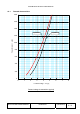
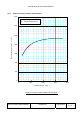
MITSUBISHI ELECTRIC CORPORATION 12-1 Forward characteristics 1800 1600 1400 Tj=125°C Tj=25°C Forward current IF [A] 1200 1000 800 600 400 200 0 0 1 2 3 4 5 6 7 8 Forward voltage VFM [V] Forward voltage characteristics (typical) HIGH VOLTAGE DIODE MODULE HVM-2018 (HV-SETSU) PAGE 6 / 11
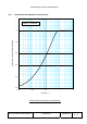
MITSUBISHI ELECTRIC CORPORATION 12-2 Reverse recovery energy characteristics 1.4 Tj = 125°C, VR = 2250V Ls = 150nH, Inductive load Integration range: 10%VR ~10%IF 1.2 Reverse recovery energy Erec [J/P] 1.0 0.8 0.6 0.4 0.2 0.
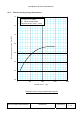
MITSUBISHI ELECTRIC CORPORATION 12-3 Reverse recovery current characteristics 1400 Tj = 125°C, VR = 2250V Ls = 150nH, Inductive load 1200 Reverse recovery current Irr [A] 1000 800 600 400 200 0 0 500 1000 1500 2000 Forward current IF [A] Reverse recovery current characteristics (typical) HIGH VOLTAGE DIODE MODULE HVM-2018 (HV-SETSU) PAGE 8 / 11
MITSUBISHI ELECTRIC CORPORATION 12-4 Transient thermal impedance characteristics 1.2 Rth(j-c) = 20 K/kW Normalized transient thermal impedance 1.0 0.8 0.6 0.4 0.2 0.0 0.001 0.01 0.1 1 10 Time [sec.
MITSUBISHI ELECTRIC CORPORATION 12-5 Reverse recovery safe operating area 2500 Tj = 125°C, VR ≤ 3000 V di/dt ≤ 2600A/µs Reverse recovery current Irr [A] 2000 1500 1000 500 0 0 1000 2000 3000 4000 5000 Reverse voltage VR [V] Reverse recovery safe operating area (RRSOA) HIGH VOLTAGE DIODE MODULE HVM-2018 (HV-SETSU) PAGE 10 / 11
MITSUBISHI ELECTRIC CORPORATION Rev. No. − Signature & date K.Kurachi 10-Apr.