
User Manual


PS21997-4, PS21997-4A
Intellimod™ Module
Dual In-line Intelligent Power Module
30 Amperes/600 Volts
Powerex, Inc., 173 Pavilion Lane, Youngwood, Pennsylvania 15697-1800 (724) 925-7272
710/09
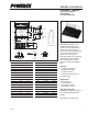
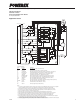
Protection Function Timing Diagrams
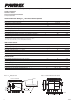
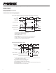
Typical Interface Circuit
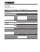
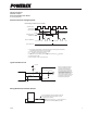
Wiring Method Around Shunt Resistor
c1
c5
c6
c3
c2
UV
DBt
c4
SET
RESETRESET
HIGH LEVEL (NO FAULT OUTPUT)
UV
DBr
CONTROL INPUT
PROTECTION
CIRCUIT STATE
CONTROL SUPPLY
VOLTAGE V
DB
OUTPUT CURRENT I
C
FAULT OUTPUT F
O
Under-Voltage Protection (P-side, UV
DB
)
c1: Control supply voltage V
DB
rises – After V
DB
level reaches under voltage reset level (UV
DBr
),
the circuits starts to operate when next input is applied.
c2: Normal operation – IGBT turns on and carries current.
c3: V
DB
level dips to under voltage trip level (UV
DBt
).
c4: P-side IGBT turns off in spite of control input signal level, but there is no F
O
signal output.
c5: V
DB
level reaches UV
DBr
.
c6: Normal operation – IGBT on and carries current.
U
P
, V
P
, W
P
, U
N
, V
N
, W
N
MCU
5V LINE
10kΩ
3.3kΩ (MIN)
F
O
V
NC
(LOGIC)
DIP-IPM
NOTE: RC coupling at each input
(parts shown dotted) may change
depending on the PWM control
scheme used in the application and
the wiring impedance of the printed
circuit board. The DIPIPM input signal
section integrates a 3.3k
Ω (min)
pull-down resistor. Therefore, when
using an external filtering resistor, care
must be taken to satisfy the turn-on
threshold voltage requirement.
V
NC
N
DIPIPM
It is recommended to make the inductance under 10nH.
For shunt resistors, it is recommended to use as low
inductance type as possible.
Shunt Resistor
Connect the wiring from V
NC
terminal at the point as
close to shunt resistors’ terminal as possible.