
Instruction Manual

PS21964-4S
Intellimod™ Module
Dual-In-Line Intelligent Power Module
15 Amperes/600 Volts
Powerex, Inc., 173 Pavilion Lane, Youngwood, Pennsylvania 15697 (724) 925-7272
7Rev. 12/09
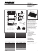
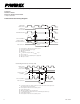
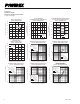
Protection Function Timing Diagrams
C1
C4
C5
C2
UV
Dt
C6
C3
SET
RESETRESET
HIGH LEVEL (NO FAULT OUTPUT)
UV
DBr
CONTROL INPUT
PROTECTION
CIRCUIT STATE
CONTROL SUPPLY
VOLTAGE V
DB
OUTPUT CURRENT I
C
FAULT OUTPUT F
O
Under-Voltage Protection (Upper-side, UV
DB
)
C1: Control supply voltage rises – After the voltage level reaches UV
DBr
, the drive circuit begins to work
at the rising edge of the next input signal.
C2: Normal operation – IGBT turn on and conducting current.
C3: Under-voltage trip (UV
DBt
).
C4: IGBT stays off regardless of the control input level, but there is no F
O
signal output.
C5: Under-voltage reset (UV
Dr
).
C6: Normal operation – IGBT turn on and conducting current.
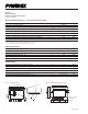
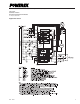
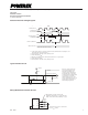
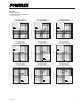
Typical Interface Circuit
Wiring Method Around Shunt Resistor
V
NC
NW
NV
NU
DIP-IPM
Wiring inductance should be less than 10nH.
(Equivalent to the inductance of a copper pattern with
length = 17mm, width = 3mm, and thickness = 100
µm.)
Shunt
Resistors
Please make the connection of shunt resistor
close to V
NC
terminal.
U
P
, V
P
, W
P
, U
N
, V
N
, W
N
MCU
5V LINE
10kΩ
3.3kΩ (MIN)
F
O
V
NC
(LOGIC)
DIP-IPM
NOTE: RC coupling at each input
(parts shown dotted) may change
depending on the PWM control
scheme used in the application and
the wiring impedance of the printed
circuit board. The DIP-IPM input signal
section integrates a 3.3k
Ω (min)
pull-down resistor. Therefore, when
using an external filtering resistor, care
must be taken to satisfy the turn-on
threshold voltage requirement.