
User Manual

PS21765
Intellimod™ Module
Dual-In-Line Intelligent Power Module
20 Amperes/600 Volts
Powerex, Inc., 173 Pavilion Lane, Youngwood, Pennsylvania 15697 (724) 925-7272
7Rev. 07/07
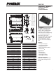
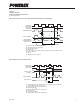
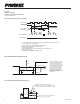
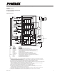
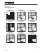
Application Circuit
Component Selection:
Dsgn. Typ. Value
Description
Notes:
D
1
1A, 600V Boot strap supply diode – Ultra fast recovery
DZ
1
16V, 0.25W Control and boot strap supply over voltage suppression
C
1
10-100uF, 50V Boot strap supply reservoir – Electrolytic, long life, low Impedance, 105°C (Note 5)
C
2
0.22-2.0uF, 50V Local decoupling/High frequency noise filters – Multilayer ceramic (Note 5)
C
3
10-100uF, 50V Control power supply filter – Electrolytic, long life, low Impedance, 105°C (Note 5)
C
4
22nF, 50V Fault output timer capacitor
C
5
100pF, 50V Optional Input signal noise filter – Multilayer ceramic (Note 1)
C
6
200-2000uF, 450V Main DC bus filter capacitor – Electrolytic, long life, high ripple current, 105°C
C
7
0.1-0.22uF, 450V Surge voltage suppression capacitor – Polyester/Polypropylene film (Note 8)
R
SHUNT
5-100mohm Current sensing resistor – Non-inductive, temperature stable, tight tolerance (Note 9)
R
1
10 ohm Boot strap supply inrush limiting resistor
R
2
330 ohm Optional control input noise filter (Note 1, Note 2)
R
3
10k ohm Fault output signal pull-up resistor (Note 3)
1) Input drive is active-high type. There is a 2.5k7(min.) pull-down resistor integrated in the IC input circuit. To prevent malfunction, the wiring
of each input should be as short as possible. When using RC coupling circuit, make sure the input signal level meets the turn-on and turn-off
threshold voltage. See application notes for details.
2) Internal HVIC provides high voltage level shifting allowing direct connection of all six driving signals to the controller.
3) F
O
output is an open collector type. Pull up resistor (R3) should be adjusted to current sink capability of the controller.
4) To prevent input signal oscillations, minimize wire length to controller (~2cm). Additional RC filtering (C5 etc.) may be required. If filtering is added
be careful to maintain proper dead time and voltage levels. See application notes for details.
5) All capacitors should be mounted as close to the terminals as possible. (C
1
: good temperature, frequency characteristic electrolytic type,
and C
2
, C
3
: good temperature, frequency and DC bias characteristic ceramic type are recommended.)
6) Shows short circuit protection disabled. See application notes for use of short circuit protection.
7) Local decoupling frequency filter capacitors must be connected as close as possible to the module’s pins.
8) The length of the DC link wiring between C5, C6, the DIP’s P terminal and the shunt must be minimized to prevent excessive transient
voltages. In particular C6 should be mounted as close to the DIP as possible.
9) Use high quality, tight tolerance current sensing resistor. Connect resistor as close as possible to the DIP’s N terminal. Be careful to check
for proper power rating. See application notes for calculation of resistance value.
10) Inserting a Zener diode (24V/1W) between each pair of control supply terminals to prevent surge destruction is recommended.
+
C
2
C
1
C
7
C
6
+
AC LINE
D
1
DZ
1
R
1
R
2
C
2
C
5
C
5
C
5
U
P
V
UFB
V
UFS
V
P1
+
C
2
C
1
D
1
R
1
R
2
C
2
V
P
V
VFB
V
VFS
V
P1
+
+
C
2
C
1
D
1
R
1
R
2
C
2
W
P
V
NO
U
N
V
N
W
N
F
O
V
WFB
V
WFS
V
P1
V
N1
V
NC
C
IN
C
FO
+15V
C
2
C
4
C
5
C
5
C
5
R
2
R
3
R
2
R
2
C
3
+3.3 to +5V
+V
CC
LVIC
FAULT
LOGIC
INPUT SIGNAL
CONDITIONING
UV
PROT.
OVER CURRENT
PROTECTION
GATE DRIVE
UV PROT.
LEVEL SHIFT
INPUT
CONDITION
HVIC
+V
CC
GATE DRIVE
UV PROT.
LEVEL SHIFT
INPUT
CONDITION
HVIC
+V
CC
GATE DRIVE
UV PROT.
LEVEL SHIFT
INPUT
CONDITION
HVIC
+V
CC
P
U
V
W
N(W)
N(V)
N(U)
R
SHUNT
MOTOR
CONTROLLER
GATE DRIVE
R
SHUNT
R
SHUNT
TO
CONTROLLER
This symbol indicates
connection to ground plane.
DZ
1
DZ
1