
User guide

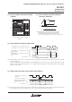


MITSUBISHI SEMICONDUCTOR <Application Specific Intelligent Power Module>
PS11011
FLAT-BASE TYPE
INSULATED TYPE
Jan. 2000
Supply voltage
∆V
DH
, ∆V
DB
VCIN(on)
VCIN(off)
fPWM
tdead
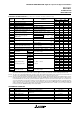
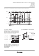
RECOMMENDED CONDITIONS
V 400 (max.)Applied across P2-N terminals
Applied between V
DH-GND, CBU+-CBU–, CBV+-CBV–,
C
BW+-CBW–
Condition
Symbol
Item Ratings
VCC
Unit
Min.
150—
Trip level
Reset level
Trip level
Reset level
Trip level
Reset level
Trip level
Reset level
Filter time
Idle
Active
t
d(read)
±IOL
ICL(H)
ICL(L)
SC
OT
OTr
UV
DH
UVDHr
OVDH
OVDHr
UVDB
UVDBr
tdV
IFO(H)
IFO(L)
tint
VCO
V
C+
(200%)
V
C–
(200%)
|∆VCO|
V
C+
VC–
∆VC(200%)
Ic = 0A
Ic = I
OP(200%)
Ic = –I
OP(200%)
Input on threshold voltage
Input off threshold voltage
Input pull-up resistor
1.87
0.77
2.97
—
—
4.0
—
—
—
3.50
100
—
11.05
11.55
18.00
16.50
10.0
10.5
—
—
—
T
C = –20°C ~ +100°C
Tj ≤ 125°C
—
1
6.00
110
90
12.00
12.50
19.20
17.50
11.0
11.5
10
—
1
V
DH = 15V
T
C = –20°C ~ +100°C
(Fig. 4)
0.8
2.5
—
2
Integrated between input terminal-VDH
TC ≤ 100°C, Tj ≤ 125°C
V
DH = 15V, TC = –20°C ~ +100°C (Note 3)
Relates to corresponding input
(Except brake part) T
C
= –20°C ~ +100°C
Relates to corresponding input (Except brake part)
ConditionSymbol
Ratings
Vth(on)
Vth(off)
Ri
fPWM
txx
Typ. Max.
Unit
ELECTRICAL CHARACTERISTICS (Tj = 25°C, VDH = 15V, VDB = 15V unless otherwise noted)
(Note 3) : (a) Allowable minimum input on-pulse width : This item applies to P-side circuit only.
(b) Allowable maximum input on-pulse width : This item applies to both P-side and N-side circuits excluding the brake circuit.
(Note4) : CL output : The "current limit warning (CL) operation circuit outputs warning signal whenever the arm current exceeds this limit. The
circuit is reset automatically by the next input signal and thus, it operates on a pulse-by-pulse scheme.
(Note5) : The short circuit protection works instantaneously when a high short circuit current flows through an internal IGBT rising up momen-
tarily. The protection function is, thus meant primarily to protect the ASIPM against short circuit distraction. Therefore, this function is
not recommended to be used for any system load current regulation or any over load control as this might, cause a failure due to
excessive temperature rise. Instead, the analogue current output feature or the over load warning feature (CL) should be appropri-
ately used for such current regulation or over load control operation. In other words, the PWM signals to the ASIPM should be shut
down, in principle, and not to be restarted before the junction temperature would recover to normal, as soon as a fault is feed back
from its F
O1 pin of the ASIPM indicating a short circuit situation.
Allowable input on-pulse width
Allowable input signal dead time for
blocking arm shoot-through
Input inter-lock sensing
Analogue signal linearity with
output current
Offset change area vs temperature
VDH = 15V, TC = –20°C ~ +100°C
Ic > I
OP(200%), VDH = 15V
(Fig. 4)
Analogue signal output voltage limit
|V
CO-VC±(200%)|
Analogue signal over all linear variation
Analogue signal data hold accuracy
After input signal trigger point (Fig. 8)
Analogue signal reading time
Current limit warning (CL) operation level
VDH =15V
Open collector output
1
2.2
—
–5
—
2.64
Open collector output
1.4
3.0
150
—
—
—
65
2.27
1.17
3.37
15
—
—
1.1
—
3
3.10
1
—
9.60
120
—
12.75
13.25
20.15
18.65
12.0
12.5
—
1
—
2.0
4.0
—
20
500
—
100
2.57
1.47
3.67
—
0.7
—
—
5
—
3.60
µA
mA
A
°C
°C
V
V
V
V
V
V
µs
µA
mA
V
V
kΩ
kHz
µs
µs
ns
V
V
V
mV
V
V
V
%
µs
A
PWM input frequency
VDH =15V, TC = –20°C ~ +100°C (Note 4)
Item
t
dead
Correspond to max. 500µs data hold period
only, Ic = I
OP(200%) (Fig. 5)
r
CH
Short circuit over current trip level
Signal output current of
CL operation
Idle
Active
Tj = 25°C (Fig. 7) (Note 5)
Supply circuit under &
over voltage protection
Over temperature protection
Fault output current
V
DH = 15V, VCIN = 5V
—mA
IDH
Circuit current
V
DH, VDB Control supply voltage
Supply voltage ripple
Input on voltage
Input off voltage
PWM Input frequency
Arm shoot-through blocking time
Using application circuit
Using application circuit
15±1.5
±1 (max.)
0 ~ 0.3
4.8 ~ 5.0
2 ~ 20
2.2 (min.)
V
V/µs
V
V
kHz
µs