
User guide


MITSUBISHI SEMICONDUCTOR <Application Specific Intelligent Power Module>
PS11011
FLAT-BASE TYPE
INSULATED TYPE
Jan. 2000
—0.1
V
CC ≤ 400V, Input = ON (one-shot)
Tj = 125°C start
13.5V ≤ V
DH = VDB ≤ 16.5V
V
CC ≤ 400V, Tj ≤ 125°C,
Ic < I
OL(CL) operation level, Input = ON
13.5V ≤ V
DH = VDB ≤ 16.5V
V
V
—
V
FBr
IRRM
VFR
ton
tc(on)
toff
tc(off)
trr
TC
7.3
6.1
7.3
6.1
4.8
0.053
Collector-emitter saturation voltage
FWDi forward voltage
Brake IGBT
Collector-emitter saturation voltage
Brake diode forward voltage
Converter diode reverse current
Converter diode voltage
Switching times
FWD reverse recovery time
V
CE(sat)
VEC
Ratings
°C/W
°C/W
°C/W
°C/W
°C/W
°C/W
—
—
—
—
—
—
Junction to case Thermal
Resistance
Condition
Symbol
Item
Ratings Unit
(Note 2)
—
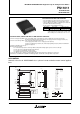
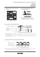
(Fig. 3)
60 Hz sinusoidal AC applied between all terminals and
the base plate for 1 minute.
Mounting screw: M3.5
T
j
Tstg
TC
Viso
—
Junction temperature
Storage temperature
Module case operating temperature
Isolation voltage
Mounting torque
–20 ~ +125
–40 ~ +125
–20 ~ +100
2500
0.78 ~ 1.27
°C
°C
°C
Vrms
kg·cm
TOTAL SYSTEM
Note 2) The item defines the maximum junction temperature for the power elements (IGBT/Diode) of the ASIPM to ensure safe operation. How-
ever, these power elements can endure junction temperature as high as 150°C instantaneously . To make use of this additional tem-
perature allowance, a detailed study of the exact application conditions is required and, accordingly, necessary information is requested
to be provided before use.
Condition
Symbol Item
Ratings
Inverter IGBT (1/6)
Inverter FWDi (1/6)
Brake IGBT
Brake FWDi
Converter Di (1/6)
Case to fin, thermal grease applied (1 Module)
Rth(j-c)
Q
Rth(j-c)F
Rth(j-c)QB
Rth(j-c)FB
Rth(j-c)
FR
Rth(c-f)
Min.
THERMAL RESISTANCE
Typ. Max.
—
—
—
—
—
—
Unit
(Fig. 3)
CASE TEMPERATURE MEASUREMENT POINT (3mm from the base surface)
VDH = VDB = 15V, Input = ON, Tj = 25°C, IC = 2A
Condition
Symbol Item
Min. Typ. Max.
Unit
• No destruction
• F
O output by protection operation
ELECTRICAL CHARACTERISTICS (Tj = 25°C, VDH = 15V, VDB = 15V unless otherwise noted)
Contact Thermal Resistance
Tj = 25°C, IC = –2A, Input = OFF
• No destruction
• No protecting operation
• No F
O output
V
CE(sat)Br VDH = 15V, Input = ON, Tj = 25°C, IC = 2A
Tj = 25°C, I
F = 2A, Input = OFF
V
R = VRRM, Tj = 125°C
Tj = 25°C, I
F = 5A
1/2 Bridge inductive load, Input = ON
V
CC = 300V, Ic = 2A, Tj = 125°C
V
DH = 15V, VDB = 15V
Note : ton, toff include delay time of the internal control
circuit
Short circuit endurance
(Output, Arm, and Load,
Short Circuit Modes)
Switching SOA
—
—
—
—
—
0.3
—
—
—
—
—
—
—
—
—
—
0.6
0.2
1.1
0.35
2.9
2.9
3.5
2.9
8
1.5
1.5
0.6
1.8
1.0
V
V
mA
V
µs
µs
µs
µs
µs