
User guide
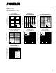


PM50RLA120
Intellimod™ L-Series
Three Phase IGBT Inverter + Brake
50 Amperes/1200 Volts
4
Powerex, Inc., 200 E. Hillis Street, Youngwood, Pennsylvania 15697-1800 (724) 925-7272
Electrical and Mechanical Characteristics, T
j
= 25°C unless otherwise specified
Characteristics Symbol Test Conditions Min. Typ. Max. Units
Control Sector
Short Circuit Trip Level SC Inverter Part 100 — — Amperes
(-20°C ≤ T
j
≤ 125°C, V
D
= 15V) Brake Part 50 — — Amperes
Short Circuit Current Delay Time t
off(SC)
V
D
= 15V — 0.2 — µs
Over Temperature Protection OT Trip Level 135 145 155 °C
(Detect T
j
of IGBT Chip) OT
R
Reset Level — 125 — °C
Supply Circuit Under-voltage Protection UV Trip Level 11.5 12.0 12.5 Volts
(-20 ≤ T
j
≤ 125°C) UV
R
Reset Level — 12.5 — Volts
Circuit Current I
D
V
D
= 15V, V
CIN
= 15V, V
N1
-V
NC
— 20 30 mA
V
D
= 15V, V
CIN
= 15V, V
XP1
-V
XPC
— 5 10 mA
Input ON Threshold Voltage V
th(on)
Applied between U
P
-V
UPC
, 1.2 1.5 1.8 Volts
Input OFF Threshold Voltage V
th(off)
V
P
-V
VPC
, W
P
-V
WPC
, U
N
- V
N
- W
N
-Br-V
NC
1.7 2.0 2.3 Volts
Fault Output Current* I
FO(H)
V
D
= 15V, V
CIN
= 15V — — 0.01 mA
I
FO(L)
V
D
= 15V, V
CIN
= 15V — 10 15 mA
Fault Output Pulse Width* t
FO
V
D
= 15V 1.0 1.8 — ms
*Fault output is given only when the internal SC, OT and UV protections schemes of either upper or lower devide operate to protect it.
Thermal Characteristics, T
j
= 25°C unless otherwise specified
Characteristic Symbol Condition Min. Typ. Max. Units
Junction to Case Thermal Resistance R
th(j-c)Q
IGBT (Per 1/6 Module) — — 0.26 °C/Watt
Inverter Part R
th(j-c)D
FWDi (Per 1/6 Module) — — 0.39 °C/Watt
Junction to Case Thermal Resistance R
th(j-c)Q
IGBT — — 0.36 °C/Watt
Brake Part R
th(j-c)D
FWDi — — 0.60 °C/Watt
Contact Thermal Resistance R
th(c-f)
Case to Fin Per Module, — — 0.038 °C/Watt
Thermal Grease Applied
Recommended Conditions for Use
Characteristic Symbol Condition Value Units
Supply Voltage V
CC
Applied across P-N Terminals ≤800 Volts
Control Supply Voltage** V
D
Applied between V
UP1
-V
UPC
, 15.0 ± 1.5 Volts
V
VP1
-V
VPC
, V
WP1
-V
WPC
,
V
N1
-V
NC
Input ON Voltage V
CIN(on)
Applied between U
P
-V
UPC
, ≤0.8 Volts
Input OFF Voltage V
CIN(off)
V
P
-V
VPC
, W
P
-V
WPC
, U
N
- V
N
- W
N
-Br-V
NC
≥9.0 Volts
PWM Input Frequency f
PWM
— ≤20 kHz
Arm Shoot-through Blocking Time t
DEAD
Input Signal ≥2.5 µs
** With ripple satisfying the following conditions: dv/dt swing ≤ ±5V/µs, Variation ≤ 2V peak to peak.