
Owner manual

PM50RL1B060
Intellimod™ L1-Series
Three Phase IGBT Inverter + Brake
50 Amperes/600 Volts
3
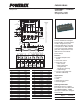
Powerex, Inc., 173 Pavilion Lane, Youngwood, Pennsylvania 15697 (724) 925-7272 www.pwrx.com
03/10 Rev. 1
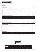
Electrical and Mechanical Characteristics, T
j
= 25°C unless otherwise specied
Characteristics Symbol Test Conditions Min. Typ. Max. Units
IGBT Inverter Sector
Collector-Emitter Saturation Voltage V
CE(sat)
V
D
= 15V, V
CIN
= 0V, I
C
= 50A, — 1.75 2.35 Volts
T
j
= 25°C
V
D
= 15V, V
CIN
= 0V, I
C
= 50A, — 1.75 2.35 Volts
T
j
= 125°C
Diode Forward Voltage V
EC
-I
C
= 50A, V
CIN
= 15V, V
D
= 15V — 1.7 2.8 Volts
Inductive Load Switching Times t
on
0.3 0.8 2.0 µs
t
rr
V
D
= 15V, V
CIN
= 0 ⇔ 15V — 0.4 0.8 µs
t
C(on)
V
CC
= 300V, I
C
= 50A — 0.4 1.0 µs
t
off
T
j
= 125°C — 1.0 2.3 µs
t
C(off)
— 0.3 1.0 µs
Collector-Emitter Cutoff Current I
CES
V
CE
= V
CES
, V
D
= 15V, T
j
= 25°C — — 1.0 mA
V
CE
= V
CES
, V
D
= 15V, T
j
= 125°C — — 10 mA
IGBT Brake Sector
Collector-Emitter Saturation Voltage V
CE(sat)
V
D
= 15V, V
CIN
= 0V, I
C
= 50A, — 1.75 2.35 Volts
T
j
= 25°C
V
D
= 15V, V
CIN
= 0V, I
C
= 50A, — 1.75 2.35 Volts
T
j
= 125°C
Forward Voltage V
FM
I
F
= 50A — 1.7 2.8 Volts
Collector-Emitter Cutoff Current I
CES
V
CE
= V
CES
, V
D
= 15V, T
j
= 25°C — — 1.0 mA
V
CE
= V
CES
, V
D
= 15V, T
j
= 125°C — — 10 mA
Control Sector
Circuit Current I
D
V
D
= 15V, V
CIN
= 15V, V
N1
-V
NC
— 8 16 mA
V
D
= 15V, V
CIN
= 15V, V
XP1
-V
XPC
— 2 4 mA
Input ON Threshold Voltage V
th(on)
Applied between U
P
-V
UPC
, 1.2 1.5 1.8 Volts
Input OFF Threshold Voltage V
th(off)
V
P
-V
VPC
, W
P
-V
WPC
, U
N
- V
N
- W
N
-Br-V
NC
1.7 2.0 2.3 Volts
Short Circuit Trip Level SC Inverter Part 100 — — Amperes
(-20°C ≤ T
j
≤ 125°C, V
D
= 15V) Brake Part 100 — — Amperes
Short Circuit Current Delay Time t
off(SC)
V
D
= 15V — 0.2 — µs
Over Temperature Protection OT Trip Level 135 — — °C
(Detect T
j
of IGBT Chip) OT
(hys)
Reset Level — 20 — °C
Supply Circuit Under-voltage Protection UV Trip Level 11.5 12.0 12.5 Volts
(-20 ≤ T
j
≤ 125°C) UV
R
Reset Level — 12.5 — Volts
Fault Output Current* I
FO(H)
V
D
= 15V, V
CIN
= 15V — — 0.01 mA
I
FO(L)
V
D
= 15V, V
CIN
= 15V — 10 15 mA
Fault Output Pulse Width* t
FO
V
D
= 15V 1.0 1.8 — ms
*Fault output is given only when the internal SC, OT and UV protections schemes of either upper or lower arm device operates to protect it.