
User Manual

www.vishay.com For technical questions, contact: indmodules@vishay.com
Document Number: 93754
2 Revision: 04-Nov-09
P100 Series
Vishay High Power Products
Passivated Assembled
Circuit Elements, 25 A
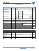
ON-STATE CONDUCTION
PARAMETER SYMBOL TEST CONDITIONS VALUES UNITS
Maximum DC output current
at case temperature
I
O
Full bridge
25 A
85 °C
Maximum peak, one-cycle
non-repetitive on-state or
forward current
I
TSM
,
I
FSM
t = 10 ms
No voltage
reapplied
Sinusoidal half wave,
initial T
J
= T
J
maximum
357
A
t = 8.3 ms 375
t = 10 ms
100 % V
RRM
reapplied
300
t = 8.3 ms 315
Maximum I
2
t for fusing I
2
t
t = 10 ms
No voltage
reapplied
637
A
2
s
t = 8.3 ms 580
t = 10 ms
100 % V
RRM
reapplied
450
t = 8.3 ms 410
Maximum I
2
√t for fusing I
2
√t
t = 0.1 ms to 10 ms, no voltage reapplied
I
2
t for time tx = I
2
√t · √tx
6365 A
2
√s
Maximum value of
threshold voltage
V
T(TO)
T
J
= 125 °C 0.82 V
Maximum level value of on-state
slope resistance
r
t1
T
J
= 125 °C, average power = V
T(TO)
x I
T(AV)
+ r
t
+ (I
T(RMS)
)
2
12 mΩ
Maximum on-state voltage drop V
TM
I
TM
= π x I
T(AV)
T
J
= 25 °C 1.35 V
Maximum forward voltage drop V
FM
I
FM
= π x I
F(AV)
Maximum non-repetitive rate of
rise of turned-on current
dI/dt
T
J
= 125 °C from 0.67 V
DRM
I
TM
= π x I
T(AV)
, I
g
= 500 mA, t
r
< 0.5 μs, t
p
> 6 μs
200 A/μs
Maximum holding current I
H
T
J
= 25 °C anode supply = 6 V, resistive load, gate open 130
mA
Maximum latching current I
L
T
J
= 25 °C anode supply = 6 V, resistive load 250
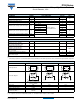
BLOCKING
PARAMETER SYMBOL TEST CONDITIONS VALUES UNITS
Maximum critical rate of rise of
off-state voltage
dV/dt T
J
= 125 °C, exponential to 0.67 V
DRM
gate open 200 V/μs
Maximum peak reverse
and off-state leakage current
at V
RRM
, V
DRM
I
RRM
,
I
DRM
T
J
= 125 °C, gate open circuit 10 mA
Maximum peak reverse
leakage current
I
RRM
T
J
= 25 °C 100 μA
RMS isolation voltage V
ISOL
50 Hz, circuit to base, all terminals shorted,
T
J
= 25 °C, t = 1 s
2500 V