
Owner manual

GT100DA60U
www.vishay.com
Vishay Semiconductors
Revision: 24-Oct-12
2
Document Number: 93185
For technical questions within your region: DiodesAmericas@vishay.com
, DiodesAsia@vishay.com, DiodesEurope@vishay.com
THIS DOCUMENT IS SUBJECT TO CHANGE WITHOUT NOTICE. THE PRODUCTS DESCRIBED HEREIN AND THIS DOCUMENT
ARE SUBJECT TO SPECIFIC DISCLAIMERS, SET FORTH AT www.vishay.com/doc?91000
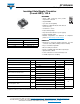
ELECTRICAL SPECIFICATIONS (T
J
= 25 °C unless otherwise specified)
PARAMETER SYMBOL TEST CONDITIONS MIN. TYP. MAX. UNITS
Collector to emitter breakdown voltage V
BR(CES)
V
GE
= 0 V, I
C
= 250 μA 600 - -
VCollector to emitter voltage V
CE(on)
V
GE
= 15 V, I
C
= 100 A - 1.72 2.0
V
GE
= 15 V, I
C
= 100 A, T
J
= 125 °C - 2.0 2.2
Gate threshold voltage V
GE(th)
V
CE
= V
GE
, I
C
= 250 μA 3.5 4.6 6.5
Temperature coefficient of
threshold voltage
V
GE(th)
/T
J
V
CE
= V
GE
, I
C
= 1 mA (25 °C to 125 °C) - - 16.8 - mV/°C
Collector to emitter leakage current I
CES
V
GE
= 0 V, V
CE
= 600 V - 0.6 100 μA
V
GE
= 0 V, V
CE
= 600 V, T
J
= 125 °C - 0.15 3 mA
Forward voltage drop V
FM
I
F
= 40 A, V
GE
= 0 V - 1.78 2.21
V
I
F
= 40 A, V
GE
= 0 V, T
J
= 125 °C - 1.39 1.74
Gate to emitter leakage current I
GES
V
GE
= ± 20 V - - ± 200 nA
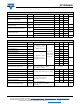
SWITCHING CHARACTERISTICS (T
J
= 25 °C unless otherwise specified)
PARAMETER SYMBOL TEST CONDITIONS MIN. TYP. MAX. UNITS
Turn-on switching loss E
on
I
C
= 100 A, V
CC
= 360 V,
V
GE
= 15 V, R
g
= 5
L = 500 μH, T
J
= 25 °C
Energy losses
include tail and
diode recovery
(see fig. 18)
-0.35-
mJ
Turn-off switching loss E
off
-2.08-
Total switching loss E
tot
-2.43-
Turn-on switching loss E
on
I
C
= 100 A, V
CC
= 360 V,
V
GE
= 15 V, R
g
= 5
L = 500 μH, T
J
= 125 °C
-0.41-
Turn-off switching loss E
off
-2.83-
Total switching loss E
tot
-3.24-
Turn-on delay time t
d(on)
- 162 -
ns
Rise time t
r
-55-
Turn-off delay time t
d(off)
- 150 -
Fall time t
f
- 129 -
Reverse bias safe operating area RBSOA
T
J
= 175 °C, I
C
= 350 A, R
g
= 22
V
GE
= 15 V to 0 V, V
CC
= 400 V,
V
P
= 600 V, L = 500 μH
Fullsquare
Diode reverse recovery time t
rr
I
F
= 50 A, dI
F
/dt = 200 A/μs, V
R
= 200 V
-6185ns
Diode peak reverse current I
rr
-47A
Diode recovery charge Q
rr
- 120 297 nC
Diode reverse recovery time t
rr
I
F
= 50 A, dI
F
/dt = 200 A/μs,
V
R
= 200 V, T
J
= 125 °C
- 133 154 ns
Diode peak reverse current I
rr
-1215A
Diode recovery charge Q
rr
- 750 1150 nC
Short circuit safe operating area SCSOA
T
J
= 175 °C, R
g
= 22 ,
V
GE
= 15 V to 0 V, V
CC
= 400 V,
V
p
= 600 V
3μs