
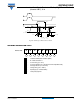
Instruction Manual

www.vishay.com For technical questions, contact: ind-modules@vishay.com
Document Number: 93011
2 Revision: 23-Apr-09
GB75DA120UP
Vishay High Power Products
Insulated Gate Bipolar Transistor
(Ultrafast IGBT), 75 A
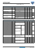
ELECTRICAL SPECIFICATIONS (T
J
= 25 °C unless otherwise specified)
PARAMETER SYMBOL TEST CONDITIONS MIN. TYP. MAX. UNITS
Collector to emitter breakdown voltage V
BR(CES)
V
GE
= 0 V, I
C
= 250 µA 1200 - -
VCollector to emitter voltage V
CE(on)
V
GE
= 15 V, I
C
= 75 A - 3.3 3.8
V
GE
= 15 V, I
C
= 75 A, T
J
= 125 °C - 3.6 3.9
Gate threshold voltage V
GE(th)
V
CE
= V
GE
, I
C
= 250 µA 4 5 6
Temperature coefficient of
threshold voltage
V
GE(th)
/ΔT
J
V
CE
= V
GE
, I
C
= 1 mA (25 °C to 125 °C) - - 12 - mV/°C
Collector to emitter leakage current I
CES
V
GE
= 0 V, V
CE
= 1200 V - 3 250 µA
V
GE
= 0 V, V
CE
= 1200 V, T
J
= 150 °C - 4 20 mA
Forward voltage drop V
FM
I
C
= 75 A, V
GE
= 0 V - 3.4 5.0
V
I
C
= 75 A, V
GE
= 0 V, T
J
= 125 °C - 3.3 5.2
Gate to emitter leakage current I
GES
V
GE
= ± 20 V - - ± 200 nA
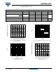
SWITCHING CHARACTERISTICS (T
J
= 25 °C unless otherwise specified)
PARAMETER SYMBOL TEST CONDITIONS MIN. TYP. MAX. UNITS
Total gate charge (turn-on) Q
g
I
C
= 50 A, V
CC
= 600 V, V
GE
= 15 V
- 690 -
nCGate to emitter charge (turn-on) Q
ge
-65-
Gate to collector charge (turn-on) Q
gc
- 250 -
Turn-on switching loss E
on
I
C
= 75 A, V
CC
= 600 V,
V
GE
= 15 V, R
g
= 5 Ω,
L = 500 µH
Energy losses
include tail and
diode recovery
(see fig. 18)
-1.53-
mJ
Turn-off switching loss E
off
-1.76-
Total switching loss E
tot
-3.29-
Turn-on switching loss E
on
I
C
= 75 A, V
CC
= 600 V,
V
GE
= 15 V, R
g
= 5 Ω,
L = 500 µH, T
J
= 125 °C
-2.49-
Turn-off switching loss E
off
-3.45-
Total switching loss E
tot
-5.94-
Turn-on delay time t
d(on)
- 281 -
ns
Rise time t
r
-45-
Turn-off delay time t
d(off)
- 300 -
Fall time t
f
- 126 -
Reverse bias safe operating area RBSOA
T
J
= 150 °C, I
C
= 200 A, R
g
= 22 Ω,
V
GE
= 15 V to 0 V, V
CC
= 900 V,
V
P
= 1200 V, L = 500 µH
Fullsquare
Diode reverse recovery time t
rr
I
F
= 50 A, dI
F
/dt = 200 A/µs, V
R
= 200 V
- 142 210 ns
Diode peak reverse current I
rr
-1316A
Diode recovery charge Q
rr
- 923 1680 nC
Diode reverse recovery time t
rr
I
F
= 50 A, dI
F
/dt = 200 A/µs,
V
R
= 200 V, T
J
= 125 °C
- 202 260 ns
Diode peak reverse current I
rr
-1822A
Diode recovery charge Q
rr
- 1818 2860 nC