
User guide

1
Target Data 03/09
GB70NA60UF
SOT 227 WARP 2
High Side Chopper
Vishay Semiconductor Italy
Revision: 13-Mar-09
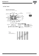
SOT-227
Absolute Maximum Ratings indicate sustained limits beyond which damage to the device may occur. All currents are
defined positive into any lead. The Thermal Resistance and Power Dissipation ratings are measured under board mounted
and still air conditions.
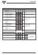
Features
Benefits
• Positive temperature coefficient
• Lower VCE (SAT)
• Lower Parasitic Capacitance
• Minimal tail current
• Tighter distribution of parameters
• Higher reliability
• Fred Hyperfast Rectifier
• Consumer electronic Power Supplies application
• Lower Conduction Losses and Switching Losses
• Higher Switching Frequency up to 150KHz
I
C(DC)
70A @ 88°C
I
F(DC)
70A @ 124°C
V
CE(on) typ
2.3V @ 70A, 25°C
V
CES
600V
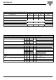
PRODUCT SUMMARY
T
J
Maximum operating junction temperature 150 °C
T
STG
Storage temperature range -55 to150
V
ISOL
RMS isolation voltage, Any terminal to case 2500 V t = 1min, TJ = 25°C
Diode
V
RRM
Repetitive peak reverse voltage 600 V
I
FM
Continuous forward current 148 A T
C
= 25°C
110 T
C
= 80°C
I
FSM
Non repetitive peak surge current 400 A T
J
= 25°C, 10 ms
P
D
Maximum power dissipation 277 W T
C
= 25°C
155 T
C
= 80°C
IGBT
V
CES
Collector to Emitter Voltage 600 V
V
GES
Gate to Emitter Voltage 20
I
CM
Pulse collector current 120 A Resistive load circuit, R = V
CC
/I
CM
I
LM
Clump inductive load current 120 A V
CC
= 480V, Vge = 15V, L = 200μH, Rg = 5Ω
I
C
Continuous collector current 111 A T
C
= 25°C
76 T
C
= 80°C
P
D
Maximum power dissipation 446 W T
C
= 25°C
250 T
C
= 80°C
PARAMETERS VALUES UNITS CONDITIONS
ABSOLUTE MAXIMUMRATINGS