
Owner's manual
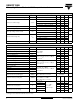
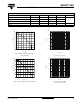
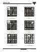
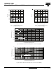
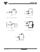
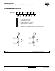
Table Of Contents
www.vishay.com For technical questions, contact: ind-modules@vishay.com
Document Number: 93653
2 Revision: 29-May-08
GB50YF120N
Vishay High Power Products
IGBT Fourpack Module, 50 A
Note
(1)
Energy losses include “tail” and diode reverse recovery
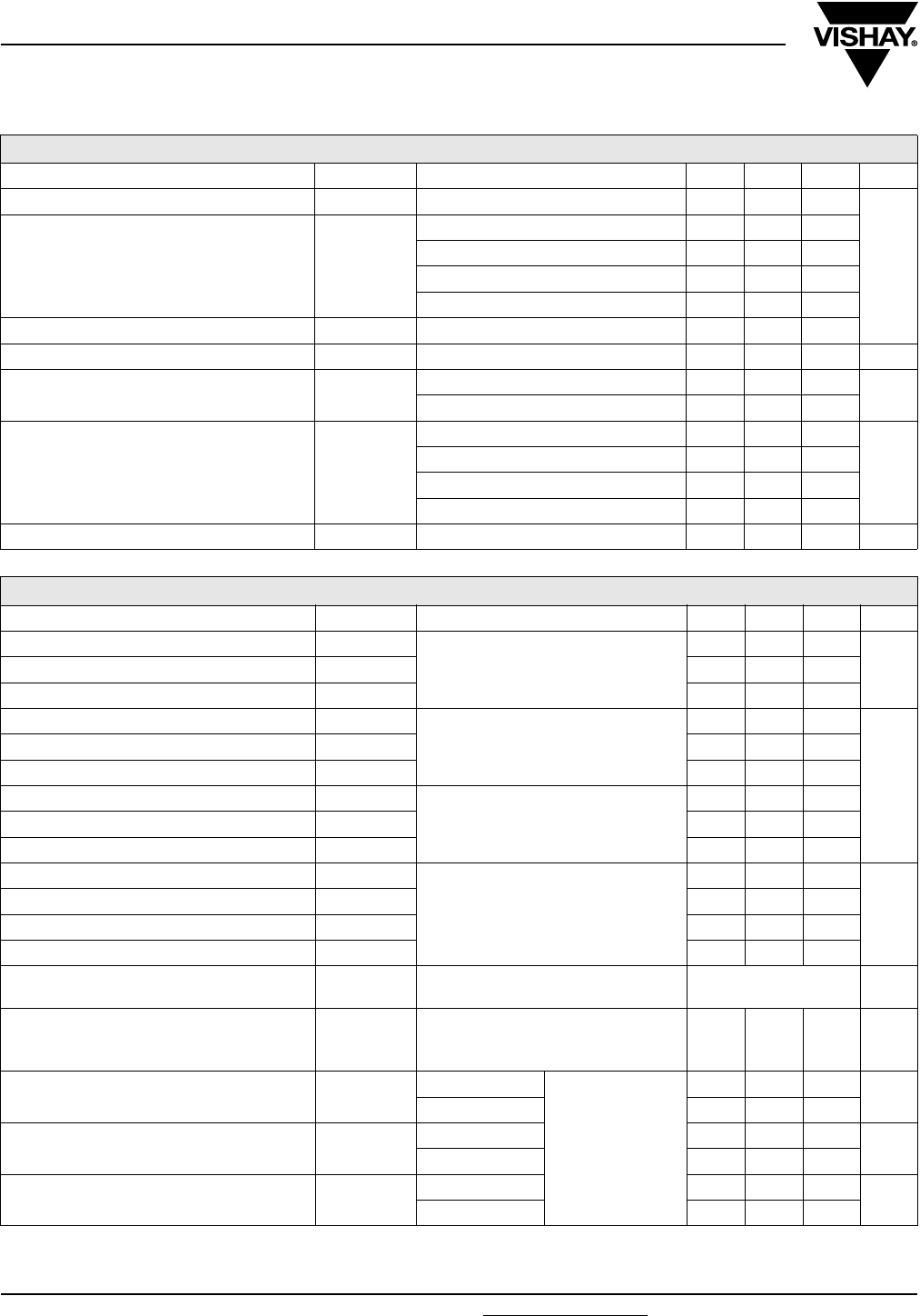
ELECTRICAL SPECIFICATIONS (T
J
= 25 °C unless otherwise specified)
PARAMETER SYMBOL TEST CONDITIONS MIN. TYP. MAX. UNITS
Collector to emitter breakdown voltage BV
(CES)
V
GE
= 0 V, I
C
= 500 µA 1200 - -
VCollector to emitter voltage V
CE(ON)
I
C
= 50 A, V
GE
= 15 V - 3.49 3.9
I
C
= 75 A, V
GE
= 15 V - 4.15 4.5
I
C
= 50 A, V
GE
= 15 V, T
J
= 125 °C - 4.16 4.5
I
C
= 75 A, V
GE
= 15 V, T
J
= 125 °C - 4.97 5.4
Gate threshold voltage V
GE(th)
V
CE
= V
GE
, I
C
= 250 µA 4.0 4.9 6.0
Threshold voltage temperature coefficient ΔV
GE(th)
/ΔT
J
V
CE
= V
GE
, I
C
= 1 mA (25 °C to 125 °C) - - 10 - mV/°C
Zero gate voltage collector current I
CES
V
GE
= 0 V, V
CE
= 1200 V - 11 250
µA
V
GE
= 0 V, V
CE
= 1200 V, T
J
= 125 °C - 600 1000
Diode forward voltage drop V
FM
I
F
= 50 A - 3.30 4.5
V
I
F
= 75 A - 3.90 5.0
I
F
= 50 A, T
J
= 125 °C - 3.6 4.8
I
F
= 75 A, T
J
= 125 °C - 4.37 5.5
Gate to emitter leakage current I
GES
V
GE
= ± 20 V - - ± 200 nA
SWITCHING CHARACTERISTICS (T
J
= 25 °C unless otherwise noted)
PARAMETER SYMBOL TEST CONDITIONS MIN. TYP. MAX. UNITS
Total gate charge (turn-on) Q
G
I
C
= 50 A
V
CC
= 600 V
V
GE
= 15 V
- 400 -
nCGate to emitter charge (turn-on) Q
GE
-43-
Gate to collector charge (turn-on) Q
GC
- 187 -
Turn-on switching loss E
on
I
C
= 50 A, V
CC
= 600 V
V
GE
= 15 V, R
G
= 4.7 Ω, L = 500 µH
T
J
= 25 °C
(1)
-0.93-
mJ
Turn-off switching loss E
off
-1.20-
Total switching loss E
tot
-2.13-
Turn-on switching loss E
on
I
C
= 50 A, V
CC
= 600 V
V
GE
= 15 V, R
G
= 4.7 Ω, L = 500 µH
T
J
= 125 °C
(1)
-1.68-
Turn-off switching loss E
off
-1.77-
Total switching loss E
tot
-3.46-
Turn-on delay time t
d(on)
I
C
= 50 A, V
CC
= 600 V
V
GE
= 15 V, R
G
= 4.7 Ω, L = 500 µH
T
J
= 125 °C
- 128 -
ns
Rise time t
r
-56-
Turn-off delay time t
d(off)
- 292 -
Fall time t
f
- 134 -
Reverse bias safe operating area RBSOA
T
J
= 150 °C, I
C
= 150 A
R
G
= 10 Ω, V
GE
= 15 V to 0 V
Fullsquare
Short circuit safe operating area SCSOA
T
J
= 150 °C
V
CC
= 900 V, V
P
= 1200 V
R
G
= 10 Ω, V
GE
= 15 V to 0 V
10 - - µs
Diode peak reverse recovery current I
rr
T
J
= 25 °C
V
CC
= 600 V
I
F
= 50 A
dI/dt = 7 A/µs
-1.32.3
A
T
J
= 125 °C - 2.0 3
Diode reverse recovery time t
rr
T
J
= 25 °C - 0.453 0.49
µs
T
J
= 125 °C - 0.74 0.82
Total reverse recovery charge Q
rr
T
J
= 25 °C - 0.12 0.3
µC
T
J
= 125 °C - 0.4 1.5