
Owner's manual

www.vishay.com For technical questions, contact: ind-modules@vishay.com
Document Number: 94502
2 Revision: 07-May-08
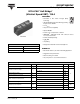
GB150TS60NPbF
Vishay High Power Products
INT-A-PAK "Half-Bridge"
(Ultrafast Speed IGBT),
138 A
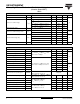
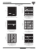
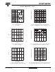
ELECTRICAL CHARACTERISTICS (T
J
= 25 °C unless otherwise specified)
PARAMETER SYMBOL TEST CONDITIONS MIN. TYP. MAX. UNITS
Collector to emitter breakdown voltage V
BR(CES)
V
GE
= 0 V, I
C
= 500 µA 600 - -
VCollector to emitter voltage V
CE(on)
V
GE
= 15 V, I
C
= 100 A - 2.2 2.7
V
GE
= 15 V, I
C
= 150 A - 2.64 3
V
GE
= 15 V, I
C
= 100 A, T
J
= 125 °C - 2.68 3.11
V
GE
= 15 V, I
C
= 150 A, T
J
= 125 °C - 3.25 3.79
Gate threshold voltage V
GE(th)
V
CE
= V
GE
, I
C
= 500 µA 3 4.2 6
Collector to emitter leakage current I
CES
V
GE
= 0 V, V
CE
= 600 V - 0.01 0.2
mA
V
GE
= 0 V, V
CE
= 600 V, T
J
= 150 °C - 7.5 15
Diode forward voltage drop V
FM
I
C
= 100 A - 1.39 1.78
V
I
C
= 150 A - 1.52 1.91
I
C
= 100 A, T
J
= 125 °C - 1.31 1.72
I
C
= 150 A, T
J
= 125 °C - 1.49 2.05
Gate to emitter leakage current I
GES
V
GE
= ± 20 V - - ± 200 nA
SWITCHING CHARACTERISTICS (T
J
= 25 °C unless otherwise specified)
PARAMETER SYMBOL TEST CONDITIONS MIN. TYP. MAX. UNITS
Turn-on switching loss E
on
I
C
= 150 A, V
CC
= 360 V, V
GE
= 15 V,
R
G
= 10 Ω, L = 200 µH
-2.0-
mJ
Turn-off switching loss E
off
-3.9-
Total switching loss E
tot
-5.9-
Turn-on switching loss E
on
I
C
= 150 A, V
CC
= 360 V, V
GE
= 15 V,
R
G
= 10 Ω, L = 200 µH, T
J
= 125 °C
-2.42-
Turn-off switching loss E
off
-4.2-
Total switching loss E
tot
-6.62-
Turn-on delay time t
d(on)
- 390 -
ns
Rise time t
r
- 100 -
Turn-off delay time t
d(off)
- 402 -
Fall time t
f
-80-
Reverse bias safe operating area RBSOA
T
J
= 150 °C, I
C
= 300 A,
R
G
= 10 Ω, V
GE
= 15 V to 0
Fullsquare
Short circuit safe operating area SCSOA
T
J
= 150 °C, V
CC
= 400 V, V
P
= 600 V,
R
G
= 10 Ω, V
GE
= 15 V to 0
10 - -
Diode reverse recovery time t
rr
I
F
= 50 A, dI
F
/dt = 200 A/µs,
V
CC
= 400 V, T
J
= 25 °C
- 226 260 ns
Diode peak reverse current I
rr
-1720A
Diode recovery charge Q
rr
- 1900 2600 nC
Diode reverse recovery time t
rr
I
F
= 50 A, dI
F
/dt = 200 A/µs,
V
CC
= 400 V, T
J
= 125 °C
- 290 330 ns
Diode peak reverse current I
rr
-2530A
Diode recovery charge Q
rr
- 3600 5000 nC