
Manual

www.vishay.com For technical questions within your region, please contact one of the following: Document Number: 93912
2 DiodesAmericas@vishay.com
, DiodesAsia@vishay.com, DiodesEurope@vishay.com Revision: 03-Aug-10
GB05XP120KTPbF
Vishay Semiconductors
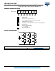
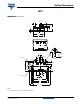
Three Phase Inverter Module in MTP Package
1200 V NPT IGBT and HEXFRED
®
Diodes, 5 A
ELECTRICAL SPECIFICATIONS (T
J
= 25 °C unless otherwise specified)
PARAMETER SYMBOL TEST CONDITIONS MIN. TYP. MAX. UNITS
Collector to emitter breakdown voltage V
(BR)CES
V
GE
= 0 V, I
C
= 250 μA 1200 - - V
Temperature coefficient of V
(BR)CES
V
(BR)CES
/T
J
V
GE
= 0 V, I
C
= 1 mA (25 °C to 125 °C) - 1.14 - V/°C
Collector to emitter voltage V
CE(on)
V
GE
= 15 V, I
C
= 6 A - 2.90 3.17
V
V
GE
= 15 V, I
C
= 12 A - 4.04 4.46
V
GE
= 15 V, I
C
= 6 A, T
J
= 125 °C - 3.45 3.60
V
GE
= 15 V, I
C
= 12 A, T
J
= 125 °C - 5.07 5.32
Gate threshold voltage V
GE(th)
I
C
= 250 μA 4 - 6
Temperature coefficient of
threshold voltage
V
GE(th)
/T
J
V
CE
= V
GE
, I
C
= 1 mA (25 °C to 125 °C) - - 10 - mV/°C
Forward transconductance g
fe
V
CE
= 25 V, I
C
= 6 A - 3.2 - S
Collector to emitter leaking current I
CES
V
GE
= 0 V, V
CE
= 1200 V - - 250
μA
V
GE
= 0 V, V
CE
= 1200 V, T
J
= 125 °C - - 1000
Diode forward voltage drop V
FM
I
F
= 6 A, V
GE
= 0 V - 2.33 2.77
V
I
F
= 12 A, V
GE
= 0 V - 3.01 3.63
I
F
= 6 A, V
GE
= 0 V, T
J
= 125 °C - 2.55 2.98
I
F
= 12 A, V
GE
= 0 V, T
J
= 125 °C - 3.45 4.07
Gate to emitter leakage current I
GES
V
GE
= ± 20 V - - ± 250 nA
SWITCHING CHARACTERISTICS (T
J
= 25 °C unless otherwise specified)
PARAMETER SYMBOL TEST CONDITIONS MIN. TYP. MAX. UNITS
Total gate charge (turn-on) Q
g
I
C
= 6 A
V
CC
= 600 V
V
GE
= 15 V
-2741
nCGate to emitter charge (turn-on) Q
ge
-3.75.6
Gate to collector charge (turn-on) Q
gc
-1421
Turn-on switching loss E
on
I
C
= 6 A, V
CC
= 600 V, V
GE
= 15 V
R
g
= 10 , L = 2.0 mH, T
J
= 25 °C
Energy losses include tail and
diode reverse recovery
- 0.606 0.909
mJTurn-off switching loss E
off
- 0.340 0.510
Total switching loss E
tot
- 0.946 1.420
Turn-on switching loss E
on
I
C
= 6 A, V
CC
= 600 V, V
GE
= 15 V
R
g
= 10 , L = 2.0 mH, T
J
= 125 °C
Energy losses include tail and
diode reverse recovery
- 0.779 1.170
mJTurn-off switching loss E
off
- 0.403 0.605
Total switching loss E
tot
- 1.182 1.775
Turn-on delay time t
d(on)
I
C
= 6 A, V
CC
= 600 V, V
GE
= 15 V
L = 2.0 mH, L
S
= 100 nH
R
g
= 10 , T
J
= 125 °C
-4771
ns
Rise time t
r
-1726
Turn-off delay time t
d(off)
- 99 150
Fall time t
f
- 362 543
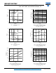
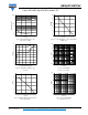
Reverse BIAS safe operating area RBSOA
T
J
= 150 °C, I
C
= 24 A
R
g
= 10 , V
GE
= 15 V to 0
Fullsquare
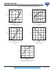
Short circuit safe operating area SCSOA
V
CC
= 600 V, V
GE
= + 15 V to 0
T
J
= 150 °C, V
P
= 1200 V, R
g
= 10
10 - - μs
Input capacitance C
ies
V
GE
= 0 V
V
CC
= 30 V
f = 1 MHz
- 369 554
pFOutput capacitance C
oes
- 244 366
Reverse transfer capacitance C
res
-1218
Diode reverse recovery energy E
rec
I
C
= 6 A, V
CC
= 600 V, V
GE
= 15 V
L = 2.0 mH, L
S
= 100 nH
R
g
= 10 , T
J
= 125 °C
- 334 - μJ
Diode reverse recovery time t
rr
-54-ns
Diode peak reverse current I
rr
-17- A