
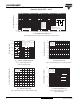
Manual

www.vishay.com For technical questions, contact: ind-modules@vishay.com
Document Number: 94363
2 Revision: 29-Apr-08
GA200SA60SP
Vishay High Power Products
Insulated Gate Bipolar Transistor
(Standard Speed IGBT), 100 A
Notes
(1)
Pulse width ≤ 80 µs; duty factor ≤ 0.1 %
(2)
Pulse width 5.0 µs, single shot
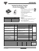
ELECTRICAL CHARACTERISTICS (T
J
= 25 °C unless otherwise noted)
PARAMETER SYMBOL TEST CONDITIONS MIN. TYP. MAX. UNITS
Collector to emitter breakdown voltage V
(BR)CES
V
GE
= 0 V, I
C
= 250 µA 600 - -
V
Emitter to collector breakdown voltage
V
(BR)ECS
(1)
V
GE
= 0 V, I
C
= 1.0 A 18 - -
Temperature coeff. of breakdown voltage ΔV
(BR)CES
/ΔT
J
V
GE
= 0 V, I
C
= 1.0 mA - 0.62 - V/°C
Collector to emitter saturation voltage V
CE(on)
I
C
= 100 A
V
GE
= 15 V
See fig. 2, 5
- 1.10 1.3
V
I
C
= 200 A - 1.33 -
I
C
= 100 A, T
J
= 150 °C - 1.02 -
Gate threshold voltage V
GE(th)
V
CE
= V
GE
, I
C
= 250 µA 3.0 - 6.0
Temperature coeff. of threshold voltage ΔV
GE(th)
/ΔT
J
V
CE
= V
GE
, I
C
= 2 mA - - 10 - mV/°C
Forward transconductance g
fe
(2)
V
CE
= 100 V, I
C
= 100 A 90 150 - S
Zero gate voltage collector current I
CES
V
GE
= 0 V, V
CE
= 600 V - - 1.0
mA
V
GE
= 0 V, V
CE
= 10 V, T
J
= 150 °C - - 10
Gate to emitter leakage current I
GES
V
GE
= ± 20 V - - ± 250 nA
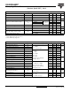
SWITCHING CHARACTERISTICS (T
J
= 25 °C unless otherwise specified)
PARAMETER SYMBOL TEST CONDITIONS MIN. TYP. MAX. UNITS
Total gate charge (turn-on) Q
g
I
C
= 100 A
V
CC
= 400 V
V
GE
= 15 V; See fig. 8
- 770 1200
nCGate emitter charge (turn-on) Q
ge
- 100 150
Gate collector charge (turn-on) Q
gc
- 260 380
Turn-on delay time t
d(on)
T
J
= 25 °C
I
C
= 100 A
V
CC
= 480 V
V
GE
= 15 V
R
G
= 2.0 Ω
Energy losses include “tail”
See fig. 9, 10, 13
-78-
ns
Rise time t
r
-56-
Turn-off delay time t
d(off)
- 890 1300
Fall time t
f
- 390 580
Turn-on switching loss E
on
-0.98-
mJTurn-off switching loss E
off
- 17.4 -
Total switching loss E
ts
- 18.4 25.5
Turn-on delay time t
d(on)
T
J
= 150 °C
I
C
= 100 A, V
CC
= 480 V
V
GE
= 15 V, R
G
= 2.0 Ω
Energy losses include “tail”
See fig. 10, 11, 13
-72-
ns
Rise time t
r
-60-
Turn-off delay time t
d(off)
-1500-
Fall time t
f
-660-
Total switching loss E
ts
- 35.7 - mJ
Internal emitter inductance L
E
Between lead, and center of
the die contact
-5.0- nH
Input capacitance C
ies
V
GE
= 0 V
V
CC
= 30 V
ƒ = 1.0 MHz; See fig. 7
- 16 250 -
pFOutput capacitance C
oes
-1040-
Reverse transfer capacitance C
res
-190-