6121 Baker Road, Suite 108 Minnetonka, MN 55345 Phone (952) 933-6190 Fax (952) 933-6223 1-800-274-4284 www.chtechnology.com Thank you for downloading this document from C&H Technology, Inc. Please contact the C&H Technology team for the following questions - Technical Application Assembly Availability Pricing Phone – 1-800-274-4284 E-Mail – sales@chtechnology.com www.chtechnology.com - SPECIALISTS IN POWER ELECTRONIC COMPONENTS AND ASSEMBLIES - www.chtechnology.
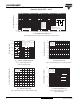
GA200SA60SP Vishay High Power Products Insulated Gate Bipolar Transistor (Standard Speed IGBT), 100 A FEATURES • Standard: Optimized for minimum saturation voltage and low operating frequencies up to 1 kHz C RoHS • Lowest conduction losses available G • Very low internal inductance (5 nH typical) • Industry standard outline E SOT-227 COMPLIANT • Fully isolated package (2500 VAC) n-channel • UL pending • Completely lead (Pb)-free • Designed and qualified for industrial level PRODUCT SUMMARY BENE
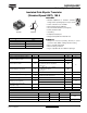
GA200SA60SP Vishay High Power Products Insulated Gate Bipolar Transistor (Standard Speed IGBT), 100 A ELECTRICAL CHARACTERISTICS (TJ = 25 °C unless otherwise noted) PARAMETER SYMBOL Collector to emitter breakdown voltage V(BR)CES Emitter to collector breakdown voltage V(BR)ECS (1) Temperature coeff. of breakdown voltage ΔV(BR)CES/ΔTJ TEST CONDITIONS MIN. TYP. MAX. VGE = 0 V, IC = 250 µA 600 - - VGE = 0 V, IC = 1.0 A 18 - - - 0.62 - VGE = 0 V, IC = 1.0 mA - 1.10 1.3 - 1.
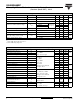
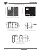
GA200SA60SP Insulated Gate Bipolar Transistor Vishay High Power Products (Standard Speed IGBT), 100 A 250 For both: Triangular wave: Duty cycle: 50 % I TJ = 125 °C Tsink = 90 °C Clamp voltage: Gate drive as specified 80 % of rated Power dissipation = 140 W Load Current (A) 200 150 Square wave: 60 % of rated voltage 100 I 50 Ideal diodes 0 1 0.1 10 100 f - Frequency (kHz) Maximum DC Collector Current (A) 1000 TJ = 150 °C 100 TJ = 25 °C 10 VGE = 15 V 20 µs pulse width 1 0.5 1.0 1.5 2.
GA200SA60SP Vishay High Power Products Insulated Gate Bipolar Transistor (Standard Speed IGBT), 100 A ZthJC - Thermal Response 1 0.1 PDM D = 0.50 D = 0.20 D = 0.10 D = 0.05 D = 0.02 D = 0.01 0.01 Single pulse (thermal resistance) 0.001 0.00001 0.0001 0.001 t1 t2 Notes: 1. Duty factor D = t1/t2 2. Peak TJ = PDM x ZthJC + TC 0.01 0.1 1 t1 - Rectangular Pulse Duration (s) Fig.
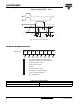
GA200SA60SP Insulated Gate Bipolar Transistor Vishay High Power Products (Standard Speed IGBT), 100 A 1000 RG = 2.0 Ω TJ = 150 °C VCC = 480 V VGE = 15 V 120 IC - Collector Current (A) Total Switching Losses (mJ) 160 80 40 VGE = 20 V TJ = 125 °C 100 10 Safe operating area 0 100 1 150 200 250 300 350 1 10 100 1000 IC - Collector Current (A) VCE - Collector to Emitter Voltage (V) Fig. 11 - Typical Switching Losses vs. Collector Current Fig. 14 - Turn-Off SOA L D.U.T.
GA200SA60SP Vishay High Power Products Insulated Gate Bipolar Transistor (Standard Speed IGBT), 100 A 1 2 90 % 10 % 3 VC 90 % td (off) 10 % 5% IC tf tr td (on) t = 5 µs Eoff Eon Ets = (Eon + Eoff) Fig.
Legal Disclaimer Notice Vishay Disclaimer All product specifications and data are subject to change without notice. Vishay Intertechnology, Inc., its affiliates, agents, and employees, and all persons acting on its or their behalf (collectively, “Vishay”), disclaim any and all liability for any errors, inaccuracies or incompleteness contained herein or in any other disclosure relating to any product.