6121 Baker Road, Suite 108 Minnetonka, MN 55345 Phone (952) 933-6190 Fax (952) 933-6223 1-800-274-4284 www.chtechnology.com Thank you for downloading this document from C&H Technology, Inc. Please contact the C&H Technology team for the following questions - Technical Application Assembly Availability Pricing Phone – 1-800-274-4284 E-Mail – sales@chtechnology.com www.chtechnology.com - SPECIALISTS IN POWER ELECTRONIC COMPONENTS AND ASSEMBLIES - www.chtechnology.
Bulletin I27201 rev. A 01/06 GA100TS60SF "HALF-BRIDGE" IGBT INT-A-PAK Standard Speed IGBT Features • • • • • VCES = 600V Standard Speed PT Igbt Technology Fred PT Antiparallel diodes with Fast recovery Very Low Conduction Losses Al2O3 DBC UL Pending IC = 220A DC VCE(on) typ. = 1.
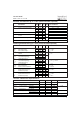
GA100TS60SF Bulletin I27201 rev. A 01/06 Electrical Characteristics @ TJ = 25°C (unless otherwise specified) Parameters Min Typ Max Units Test Conditions VBRCES Collector-to-Emitter Breakdown Voltage 600 V CE(on) Collector-to-Emitter Voltage V 1.11 V GE = 0V, I C = 1mA 1.28 V GE = 15V, I C = 100A 1.22 6 V GE = 15V, I C = 100A, T J = 125°C I C = 0.25mA 1.39 IC = 200A 1.
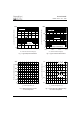
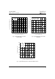
GA100TS60SF Bulletin I27201 rev. A 01/06 1000 1000 IC , Collector-to-Emitter Current (A) IC, Collector-to-Emitter Current (A) Vge = 15V 100 Tj = 25˚C Tj = 125˚C 10 0.6 0.8 1 1.2 1.4 1.6 T J = 25˚C 10 Vce = 10V 380µs PULSE WIDTH 6.5 7.5 8.5 VCE, Collector-to-Emitter Voltage (V) VGE, Gate-to-Emitter Voltage (V) Fig. 1 - Typical Output Characteristics Fig. 2 - Typical Transfer Characteristics 1.5 VCE, Collector-to-Emitter Voltage (V) Maximum DC Collector Current (A) 100 1 5.5 1.
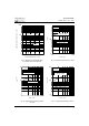
GA100TS60SF Bulletin I27201 rev. A 01/06 35 Vcc = 400V Ic = 100A Tj = 25˚C, Vce = 480V 30 Vge = 15V, Ic = 100A 15 Switching Losses (mJ) VGE, Gate-to-Emitter Voltage (V) 20 10 5 Eoff 25 20 15 Eon 10 5 0 0 100 200 300 400 500 600 700 0 10 20 30 40 50 QG, Total Gate Charge (nC) RG, Gate Reistance (Ω) Fig. 5 - Typical Gate Charge vs. Gate-toEmitter Voltage Fig.
GA100TS60SF Bulletin I27201 rev. A 01/06 1000 1000 If = 50A, Tj = 125˚C Tj = 125˚C 100 t rr (ns) Instantaneous Forward Current - I F (A) Vr = 200V 100 If = 50A, Tj = 25˚C 10 Tj = 25˚C 1 0 0.5 1 1.5 2 10 100 2.5 Forward Voltage Drop- VFM (V) di f /dt - A/µs Fig. 8 - Maximum Forward Voltage Drop vs. Instantaneous Forward Current Fig. 9 - Typical Reverse Recovery vs.
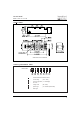
GA100TS60SF Bulletin I27201 rev. A 01/06 Outline Table All dimensions are in millimeters Ordering Information Table Device Code GA 100 1 Document Number: 93619 2 T S 60 S F 3 4 5 6 7 1 - Essential Part Number IGBT modules 2 - Current rating 3 - Circuit Configuration (T = Half Bridge) 4 - Int-A-Pak 5 - Voltage Code (60 = 600V) 6 - Speed/ Type (S = Standard Speed IGBT) 7 - Diode Type (100 = 100A) www.vishay.
GA100TS60SF Bulletin I27201 rev. A 01/06 Data and specifications subject to change without notice. This product has been designed for Industrial Level. Qualification Standards can be found on IR's Web site. IR WORLD HEADQUARTERS: 233 Kansas St., El Segundo, California 90245, USA Tel: (310) 252-7105 TAC Fax: (310) 252-7309 01/06 Document Number: 93619 www.vishay.
Legal Disclaimer Notice Vishay Notice The products described herein were acquired by Vishay Intertechnology, Inc., as part of its acquisition of International Rectifier’s Power Control Systems (PCS) business, which closed in April 2007. Specifications of the products displayed herein are pending review by Vishay and are subject to the terms and conditions shown below. Specifications of the products displayed herein are subject to change without notice. Vishay Intertechnology, Inc.