6121 Baker Road, Suite 108 Minnetonka, MN 55345 Phone (952) 933-6190 Fax (952) 933-6223 1-800-274-4284 www.chtechnology.com Thank you for downloading this document from C&H Technology, Inc. Please contact the C&H Technology team for the following questions - Technical Application Assembly Availability Pricing Phone – 1-800-274-4284 E-Mail – sales@chtechnology.com www.chtechnology.com - SPECIALISTS IN POWER ELECTRONIC COMPONENTS AND ASSEMBLIES - www.chtechnology.
VS-EMF050J60U www.vishay.com Vishay Semiconductors 3-Levels Half-Bridge Inverter Stage, 60 A/57 A FEATURES • Warp1 and Warp2 PFC IGBT • FRED Pt® and HEXFRED® antiparallel diodes • FRED Pt® clamping diodes • Integrated thermistor • Square RBSOA EMIPAK2 • Operating frequency 60 kHz to 150 kHz • Low internal inductances PRODUCT SUMMARY • Low switching loss 1° LEVEL OF HALF-BRIDGE • Compliant to RoHS Directive 2002/95/EC VCES 600 V VCE(ON) typical at IC = 50 A 1.
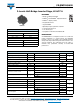
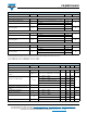
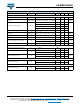
VS-EMF050J60U www.vishay.com Vishay Semiconductors ABSOLUTE MAXIMUM RATINGS PARAMETER SYMBOL TEST CONDITIONS MAX.
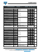
VS-EMF050J60U www.vishay.com Vishay Semiconductors ELECTRICAL SPECIFICATIONS (TJ = 25 °C unless otherwise noted) PARAMETER SYMBOL TEST CONDITIONS MIN. TYP. MAX. UNITS 900 - - V VGE = 0 V, IC = 500 μA (25 °C to 125 °C) - - 8.5 - V/°C VGE = 15 V, IC = 27 A - 2.45 2.8 VGE = 15 V, IC = 50 A - 2.73 3.2 VGE = 15 V, IC = 27 A, TJ = 125 °C - 2 2.
VS-EMF050J60U www.vishay.com Vishay Semiconductors SWITCHING CHARACTERISTICS (TJ = 25 °C unless otherwise noted) PARAMETER SYMBOL TEST CONDITIONS MIN. TYP. MAX. UNITS Q1 - Q4 IGBT (WITH FREEWHEELING D1 - D2 CLAMPING DIODE) Total gate charge (turn-on) Qg IC = 70 A - 480 720 Gate to ermitter charge (turn-on) Qge VCC = 400 V - 82 164 Gate to collector charge (turn-on) Qgc VGE = 15 V - 160 260 Turn-on switching loss EON - 0.11 - Turn-off switching loss EOFF - 0.
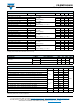
VS-EMF050J60U www.vishay.com Vishay Semiconductors SWITCHING CHARACTERISTICS (TJ = 25 °C unless otherwise noted) PARAMETER SYMBOL TEST CONDITIONS MIN. TYP. MAX. UNITS ns D1 - D2 CLAMPING DIODE Diode reverse recovery time trr Diode peak reverse current Irr Diode recovery charge Qrr Diode reverse recovery time trr Diode peak reverse current Irr Diode recovery charge Qrr VR = 200 V IF = 30 A dl/dt = 500 A/μs - 50 80 - 7.
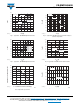
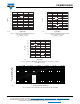
VS-EMF050J60U www.vishay.com Vishay Semiconductors 100 4.0 VGE = 15 V 90 VGE = 15 V TJ = 125 °C 3.5 80 TJ = 150 °C 50 TJ = 25 °C 40 VCE (V) 60 IC (A) 100 A 3.0 70 30 2.5 50 A 2.0 1.5 27 A 20 1.0 10 0 0.5 0 0.5 1.0 1.5 2.0 2.5 3.0 3.5 VCE (V) 93494_01 10 100 160 100 TJ = 125 °C 90 VCE = 20 V 90 80 80 70 70 50 40 60 ICE (A) VGE = 8 V VGE = 10 V VGE = 12 V VGE = 15 V VGE = 18 V 60 IC (A) 110 TJ (°C) Fig.
VS-EMF050J60U www.vishay.com Vishay Semiconductors Allowable Case Temperature (°C) 1000 100 IC (A) 10 1 0.1 160 140 120 100 DC 80 60 40 20 0.01 0 1 10 100 1000 VCE (V) 93494_07 0 5 10 15 20 25 30 35 40 45 50 IF - Continuous Forward Current (A) 93494_10 Fig. 10 - Maximum DC D5 - D6 Antiparallel Diode Forward Current vs. Case Temperature per Junction Fig. 7 - Q1 - Q4 IGBT Reverse Bias SOA TJ = 150 °C, VGE = 15 V, Rg = 22 1 1.8 1.6 1.4 125 °C Energy (mJ) ICES (mA) 0.1 0.
VS-EMF050J60U www.vishay.com Vishay Semiconductors 160 21 150 19 140 17 130 125 °C 15 110 100 90 125 °C 13 Irr (A) trr (ns) 120 11 9 80 7 70 25 °C 5 25 °C 60 3 50 40 100 200 300 400 1 100 500 dIF/dt (A/μs) 93494_13 200 Fig. 13 - Typical D5 - D6 Antiparallel Diode Reverse Recovery Time vs. dIF/dt VR = 200 V, IF = 30 A 300 400 500 dIF/dt (A/μs) 93494_14 Fig. 14 - Typical D5 - D6 Antiparallel Diode Reverse Recovery Current vs.
VS-EMF050J60U www.vishay.com Vishay Semiconductors ZthJC - Thermal Impedance Junction to Case (°C/W) 10 1 D = 0.50 D = 0.20 D = 0.10 D = 0.05 D = 0.02 D = 0.01 DC 0.1 0.01 0.001 0.00001 0.0001 0.001 0.01 0.1 1 10 t1 - Rectangular Pulse Duration (s) 93494_17 Fig.
VS-EMF050J60U www.vishay.com Vishay Semiconductors 100 10 VCE = 20 V 90 80 125 °C 1 ICES (mA) 70 ICE (A) 60 TJ = 125 °C 50 TJ = 25 °C 40 0.1 0.01 30 25 °C 20 0.001 10 0 4 5 6 7 8 VGE (V) 93494_22 0.0001 100 9 200 300 400 Fig. 22 - Typical Q1 - Q4 IGBT Transfer Characteristics 500 600 700 800 900 VCES (V) 93494_25 Fig. 25 - Typical Q2 - Q3 IGBT Zero Gate Voltage Collector Current 5.5 100 90 5.0 TJ = 25 °C TJ = 25 °C 80 4.
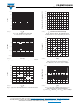
VS-EMF050J60U www.vishay.com Vishay Semiconductors 4.2 280 3.8 260 3.4 240 220 Eoff 2.6 trr (ns) Energy (mJ) 3.0 2.2 1.8 125 °C 200 180 160 1.4 1.0 140 Eon 25 °C 120 0.6 0.2 10 20 30 40 50 60 70 80 100 100 90 IC (A) 93494_28 200 Fig. 28 - Typical Q2 - Q3 IGBT Energy Loss vs. IC (with Freewheeling D2 - D3 AP Diode) VCC = 720 V, Rg = 4.7 , VGE = 15 V, L = 500 μH 300 400 500 dIF/dt (A/μs) 93494_30 Fig. 30 - Typical D3 - D4 Antiparallel Diode Reverse Recovery Time vs.
VS-EMF050J60U www.vishay.com Vishay Semiconductors ZthJC - Thermal Impedance Junction to Case (°C/W) 1 0.1 D = 0.50 D = 0.20 D = 0.10 D = 0.05 D = 0.02 D = 0.01 DC 0.01 0.001 0.00001 0.0001 0.001 0.01 0.1 1 10 t1 - Rectangular Pulse Duration (s) 93494_33 Fig. 33 - Maximum Thermal Impedance ZthJC Characteristics (Q2 - Q3 IGBT) ZthJC - Thermal Impedance Junction to Case (°C/W) 10 1 0.1 D = 0.50 D = 0.20 D = 0.10 D = 0.05 D = 0.02 D = 0.01 DC 0.01 0.001 0.00001 0.0001 0.001 0.01 0.
VS-EMF050J60U www.vishay.com Vishay Semiconductors 10 21 19 1 17 15 0.1 125 °C 13 Irr (A) IR (mA) 125 °C 11 0.01 9 7 25 °C 0.001 25 °C 5 3 0.0001 100 200 300 400 500 1 100 600 VR (V) 93494_37 200 Fig. 37 - Typical D1 - D2 Clamping Diode Reverse Leakage Current 300 400 500 dIF/dt (A/μs) 93494_39 Fig. 39 - Typical D1 - D2 Clamping Diode Reverse Recovery Current vs.
VS-EMF050J60U www.vishay.com Vishay Semiconductors ORDERING INFORMATION TABLE Device code VS- EM F 050 J 60 U 1 2 3 4 5 6 7 1 - Vishay Semiconductors product 2 - Package indicator (EM = EMIPAK2) 3 - Circuit configuration (F = 3-levels half-bridge inverter stage) 4 - Current rating (050 = 50 A) 5 - Die technology (J = Warp2 IGBT) 6 - Voltage rating (60 = 600 V) 7 - U = Ultrafast TYPICAL CONNECTION Note • Please refer to lead assignment for correct pin configuration.
VS-EMF050J60U www.vishay.com Vishay Semiconductors CIRCUIT CONFIGURATION + 400 V 17 35 Q1 D5 Inv_Drv1 9 33 D1 11 Q2 D3 Inv_Drv2 8 4 14 15 MID Q3 D4 3 Inv_Drv3 29 D2 2 30 VMID 36 Q4 1 D6 Inv_Drv3 - 400 V 23 5 24 Th 26 6 27 PACKAGE 6 5 3 2 1 4 8 14 15 9 11 33 29 36 30 24 23 17 35 26 27 LINKS TO RELATED DOCUMENTS Dimensions Revision: 09-Dec-11 www.vishay.com/doc?95436 Document Number: 93494 15 For technical questions within your region: DiodesAmericas@vishay.
Outline Dimensions Vishay Semiconductors EMIPAK2 DIMENSIONS in millimeters 15.2 12.7 8.9 Front view 55 ± 0.3 Pins position with tolerance Ø 1 ± 0.1 M4 Ø 0.4 5.1 14 11.4 10.2 7.6 7.6 6.4 3.8 2.6 1.3 13.3 3.2 1.9 1.3 5.1 2.5 6.3 Detail “A” Scale 10:1 Detail “A” 5° F 14 F 7 15.9 12.1 8.3 5.7 39 ± 0.3 5 62 ± 0.3 41.5 23 53 62 ± 0.3 Ø2 Ø 12.1 20.5 ± 1 3 ref. Top view 9.5 9.5 15.9 10.8 Side view 7 Ø 4.3 5.7 1.9 12 20.5 ± 1 17 ± 1 3.8 16.8 8.9 10.1 12.7 11.4 16.5 16.5 20.
Legal Disclaimer Notice www.vishay.com Vishay Disclaimer ALL PRODUCT, PRODUCT SPECIFICATIONS AND DATA ARE SUBJECT TO CHANGE WITHOUT NOTICE TO IMPROVE RELIABILITY, FUNCTION OR DESIGN OR OTHERWISE. Vishay Intertechnology, Inc., its affiliates, agents, and employees, and all persons acting on its or their behalf (collectively, “Vishay”), disclaim any and all liability for any errors, inaccuracies or incompleteness contained in any datasheet or in any other disclosure relating to any product.