6121 Baker Road, Suite 108 Minnetonka, MN 55345 Phone (952) 933-6190 Fax (952) 933-6223 1-800-274-4284 www.chtechnology.com Thank you for downloading this document from C&H Technology, Inc. Please contact the C&H Technology team for the following questions - Technical Application Assembly Availability Pricing Phone – 1-800-274-4284 E-Mail – sales@chtechnology.com www.chtechnology.com - SPECIALISTS IN POWER ELECTRONIC COMPONENTS AND ASSEMBLIES - www.chtechnology.
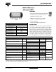
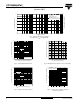
CPV363M4UPbF Vishay High Power Products IGBT SIP Module (Ultrafast IGBT) FEATURES • Fully isolated printed circuit board mount package • Switching-loss rating includes all “tail” losses RoHS • HEXFRED® soft ultrafast diodes COMPLIANT • Optimized for medium speed 1 to 10 kHz See fig. 1 for current vs. frequency curve IMS-2 • Totally lead (Pb)-free • Designed and qualified for industrial level PRODUCT SUMMARY OUTPUT CURRENT IN A TYPICAL 20 kHz MOTOR DRIVE IRMS per phase (2.
CPV363M4UPbF IGBT SIP Module (Ultrafast IGBT) Vishay High Power Products THERMAL AND MECHANICAL SPECIFICATIONS PARAMETER Junction to case, each IGBT, one IGBT in conduction Junction to case, each DIODE, one DIODE in conduction Case to sink, flat, greased surface SYMBOL TYP. MAX. RthJC (IGBT) - 3.5 UNITS RthJC (DIODE) - 5.5 RthCS (MODULE) 0.10 - 20 - g 0.7 - oz.
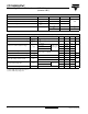
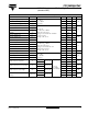
CPV363M4UPbF IGBT SIP Module (Ultrafast IGBT) Vishay High Power Products SWITCHING CHARACTERISTICS (TJ = 25 °C unless otherwise specified) PARAMETER SYMBOL Total gate charge (turn-on) Qg Gate to emitter charge (turn-on) Qge Gate to collector charge (turn-on) Qgc Turn-on delay time td(on) Rise time Turn-off delay time Fall time tr td(off) tf Turn-on switching loss Eon Turn-off switching loss Eoff Total switching loss Ets Turn-on delay time td(on) Rise time Turn-off delay time Fall time
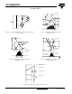
CPV363M4UPbF IGBT SIP Module (Ultrafast IGBT) Vishay High Power Products Tc = 90°C Tj = 125°C Power Factor = 0.8 Modulation Depth = 1.15 Vcc = 50% of Rated Voltage LOAD CURRENT (A) 10 2.92 8 2.33 6 1.75 4 1.17 2 0.58 Total Output Power (kW) 3.50 12 0.00 0 0.1 1 10 100 f, Frequency (KHz) Fig. 1 - Typical Load Current vs. Frequency (Load Current = IRMS of Fundamental) 14 10 TJ = 150°C TJ = 25°C 1 VGE = 15V 20µs PULSE WIDTH 0.1 0.
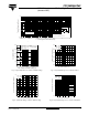
CPV363M4UPbF IGBT SIP Module (Ultrafast IGBT) Vishay High Power Products Thermal Response (Z thJC ) 10 D = 0.50 1 0.20 0.10 0.05 P DM 0.02 0.01 0.1 t 1 t SINGLE PULSE (THERMAL RESPONSE) Notes: 1. Duty factor D = t 1 /t 2 2 2. Peak TJ = P DM x Z thJC + T C 0.01 0.00001 0.0001 0.001 0.01 0.1 1 10 t 1 , Rectangular Pulse Duration (sec) Fig. 6 - Maximum Effective Transient Thermal Impedance, Junction to Case 0.
CPV363M4UPbF IGBT SIP Module (Ultrafast IGBT) Vishay High Power Products RG TJ V 1.0 CC VGE 100 = 23 Ω = 150 °C = 480V = 15V I C, Collector-to-Emitter Current (A) Total Switching Losses (mJ) 1.2 0.8 0.6 0.4 0.2 VGE = 20V o T J = 125 C 10 1 SAFE OPERATING AREA 0.0 0 2 4 6 8 10 12 14 0.1 16 1 I C , Collector-to-emitter Current (A) 10 100 1000 VCE , Collector-to-Emitter Voltage (V) Fig. 11 - Typical Switching Losses vs. Collector to Emitter Current Fig.
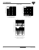
CPV363M4UPbF IGBT SIP Module (Ultrafast IGBT) Vishay High Power Products 600 160 VR = 200V TJ = 125°C TJ = 25°C VR = 200V TJ = 125°C TJ = 25°C 120 400 Q RR - (nC) t rr - (ns) I F = 24A I F = 12A 80 I F = 6.0A I F = 24A I F = 12A 200 40 IF = 6.0A 0 100 di f /dt - (A/µs) 0 100 1000 Fig. 14 - Typical Reverse Recovery Time vs. dIF/dt Fig. 16 - Typical Stored Charge vs.
CPV363M4UPbF Vishay High Power Products IGBT SIP Module (Ultrafast IGBT) GATE VOLTAGE D.U.T. 10% +Vg Same type device as D.U.T. +Vg DUT VOLTAGE AND CURRENT Vce 80 % of VCE 430 µF 10% Ic Vcc Ipk 90% Ic Ic D.U.T. 5% Vce tr td(on) t2 Eon = Vce ie dt t1 ∫ t1 Fig. 18a - Test Circuit for Measurements of ILM, Eon, Eoff(diode), trr, Qrr, Irr, td(on), tr, td(off), tf t2 Fig. 18c - Test Waveforms for Circuit of Fig.
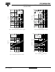
CPV363M4UPbF IGBT SIP Module (Ultrafast IGBT) D.U.T. L 1000 V Vishay High Power Products RL = VC 480 V 4 x IC at 25 °C 0 - 480 V 6000 µF 100 V 50 V Fig. 19 - Clamped Inductive Load Test Circuit Fig. 20 - Pulsed Collector Current Test Circuit CIRCUIT CONFIGURATION 1 3 Q1 D1 9 Q3 D3 4 6 Q2 D2 7 12 15 Q5 D5 10 Q4 D4 13 18 16 Q6 D6 19 LINKS TO RELATED DOCUMENTS Dimensions Document Number: 94486 Revision: 01-Sep-08 http://www.vishay.
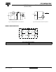
Outline Dimensions Vishay High Power Products IMS-2 (SIP) DIMENSIONS in millimeters (inches) Case Outline - IMS-2 Ø 3.91 (0.154) 2x 62.43 (2.458) 7.87 (0.310) 53.85 (2.120) 5.46 (0.215) 21.97 (0.865) 1 2 3 4 5 6 7 8 9 10 11 12 13 14 15 16 17 18 19 0.38 (0.015) 3.94 (0.155) 1.27 (0.050) 4.06 ± 0.51 (0.160 ± 0.020) 5.08 (0.200) 6x 1.27 (0.050) 13 x 2.54 (0.100) 6x 3.05 ± 0.38 (0.120 ± 0.015) 0.76 (0.030) 13 x 0.51 (0.020) 6.10 (0.
Legal Disclaimer Notice Vishay Disclaimer All product specifications and data are subject to change without notice. Vishay Intertechnology, Inc., its affiliates, agents, and employees, and all persons acting on its or their behalf (collectively, “Vishay”), disclaim any and all liability for any errors, inaccuracies or incompleteness contained herein or in any other disclosure relating to any product.