
Owner's manual


336
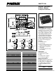
CM50TF-24H
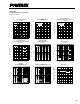
Six-IGBT IGBTMOD™ H-Series Module
50 Amperes/1200 Volts
Powerex, Inc., 200 Hillis Street, Youngwood, Pennsylvania 15697-1800 (724) 925-7272
Absolute Maximum Ratings, T
j
= 25 °C unless otherwise specified
Ratings Symbol CM50TF-24H Units
Junction Temperature T
j
–40 to 150 °C
Storage Temperature T
stg
–40 to 125 °C
Collector-Emitter Voltage (G-E SHORT) V
CES
1200 Volts
Gate-Emitter Voltage V
GES
±20 Volts
Collector Current I
C
50 Amperes
Peak Collector Current I
CM
100* Amperes
Diode Forward Current I
F
50 Amperes
Diode Forward Surge Current I
FM
100* Amperes
Power Dissipation P
d
400 Watts
Max. Mounting Torque M4 Mounting Screws – 13 in-lb
Max. Mounting Torque M5 Mounting Screws – 17 in-lb
Module Weight (Typical) – 540 Grams
V Isolation V
RMS
2500 Volts
* Pulse width and repetition rate should be such that device junction temperature does not exceed the device rating.
Static Electrical Characteristics, T
j
= 25 °C unless otherwise specified
Characteristics Symbol Test Conditions Min. Typ. Max. Units
Collector-Cutoff Current I
CES
V
CE
= V
CES
, V
GE
= 0V – – 1.0 mA
Gate Leakage Current I
GES
V
GE
= V
GES
, V
CE
= 0V – – 0.5
m
A
Gate-Emitter Threshold Voltage V
GE(th)
I
C
= 5mA, V
CE
= 10V 4.5 6.0 7.5 Volts
Collector-Emitter Saturation Voltage V
CE(sat)
I
C
= 50A, V
GE
= 15V – 2.5 3.4** Volts
I
C
= 50A, V
GE
= 15V, T
j
= 150°C – 2.25 – Volts
Total Gate Charge Q
G
V
CC
= 600V, I
C
= 50A, V
GS
= 15V – 250 – nC
Diode Forward Voltage V
FM
I
E
= 50A, V
GS
= 0V – – 3.4 Volts
** Pulse width and repetition rate should be such that device junction temperature rise is negligible.
Dynamic Electrical Characteristics, T
j
= 25 °C unless otherwise specified
Characteristics Symbol Test Conditions Min. Typ. Max. Units
Input Capacitance C
ies
–– 10nF
Output Capacitance C
oes
V
GE
= 0V, V
CE
= 10V, f = 1MHz – – 3.5 nF
Reverse Transfer Capacitance C
res
– – 2 nF
Resistive Turn-on Delay Time t
d(on)
– – 80 ns
Load Rise Time t
r
V
CC
= 600V, I
C
= 50A, – – 200 ns
Switching Turn-off Delay Time t
d(off)
V
GE1
= V
GE2
= 15V, R
G
= 6.3Ω – – 150 ns
Times Fall Time t
f
– – 350 ns
Diode Reverse Recovery Time t
rr
I
E
= 50A, di
E
/dt = –100A/
µ
s – – 250 ns
Diode Reverse Recovery Charge Q
rr
I
E
= 50A, di
E
/dt = –100A/
µ
s – 0.37 –
µ
C
Thermal and Mechanical Characteristics, T
j
= 25 °C unless otherwise specified
Characteristics Symbol Test Conditions Min. Typ. Max. Units
Thermal Resistance, Junction to Case R
th(j-c)
Per IGBT – – 0.31 °C/W
Thermal Resistance, Junction to Case R
th(j-c)
Per FWDi – – 0.70 °C/W
Contact Thermal Resistance R
th(c-f)
Per Module, Thermal Grease Applied – – 0.033 °C/W