
Owner's manual

Mar. 2003
MITSUBISHI HVIGBT MODULES
CM400DY-50H
HIGH POWER SWITCHING USE
INSULATED TYPE
HVIGBT MODULES (High Voltage Insulated Gate Bipolar Transistor Modules)
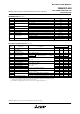
MAXIMUM RATINGS (Tj = 25°C)
VGE = 0V
V
CE = 0V
DC, T
C = 80°C
Pulse (Note 1)
Pulse (Note 1)
T
C = 25°C, IGBT part
—
—
Charged part to base plate, rms, sinusoidal, AC 60Hz 1min.
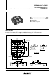
Main terminals screw M8
Mounting screw M6
Auxiliary terminals screw M4
Typical value
2500
±20
400
800
400
800
3400
–40 ~ +150
–40 ~ +125
6000
6.67 ~ 13.00
2.84 ~ 6.00
0.88 ~ 2.00
1.5
V
V
A
A
A
A
W
°C
°C
V
N·m
N·m
N·m
kg
Collector-emitter voltage
Gate-emitter voltage
Maximum collector dissipation
Junction temperature
Storage temperature
Isolation voltage
Mounting torque
Mass
Collector current
Emitter current
Symbol Item Conditions UnitRatings
V
CES
VGES
IC
ICM
IE
(Note 2)
IEM
(Note 2)
PC
(Note 3)
Tj
Tstg
Viso
—
—
V
V
V
CE = VCES, VGE = 0V
V
GE = VGES, VCE = 0V
T
j = 25°C
T
j = 125°C
V
CC = 1250V, IC = 400A, VGE = 15V
V
CC = 1250V, IC = 400A
V
GE1 = VGE2 = 15V
R
G = 7.5Ω
Resistive load switching operation
I
E = 400A, VGE = 0V
I
E = 400A
die / dt = –800A / µs
Junction to case, IGBT part (Per 1/2 module)
Junction to case, FWDi part (Per 1/2 module)
Case to fin, conductive grease applied (Per 1/2 module)
IC = 40mA, VCE = 10V
I
C = 400A, VGE = 15V (Note 4)
V
CE = 10V
V
GE = 0V
5
0.5
4.16
—
—
—
—
—
1.00
2.00
2.00
1.00
3.77
1.20
—
0.036
0.072
—
mA
µA
nF
nF
nF
µC
µs
µs
µs
µs
V
µs
µC
K/W
K/W
K/W
—
—
3.20
3.60
40
4.4
1.3
1.8
—
—
—
—
2.90
—
85
—
—
0.016
—
—
—
—
—
—
—
—
—
—
—
—
—
—
—
—
—
—
6.04.5 7.5
Collector cutoff current
Gate-emitter
threshold voltage
Gate-leakage current
Collector-emitter
saturation voltage
Input capacitance
Output capacitance
Reverse transfer capacitance
Total gate charge
Turn-on delay time
Turn-on rise time
Turn-off delay time
Turn-off fall time
Emitter-collector voltage
Reverse recovery time
Reverse recovery charge
Contact thermal resistance
Min Typ Max
I
CES
IGES
Cies
Coes
Cres
QG
td (on)
tr
td (off)
tf
VEC
(Note 2)
trr
(Note 2)
Qrr
(Note 2)
Rth(j-c)Q
Rth(j-c)R
Rth(c-f)
ELECTRICAL CHARACTERISTICS (Tj = 25°C)
Symbol
Parameter Conditions
V
GE(th)
VCE(sat)
Limits
Unit
Note 1. Pulse width and repetition rate should be such that the device junction temp. (Tj) does not exceed Tjmax rating.
2. I
E, VEC, trr, Qrr & die/dt represent characteristics of the anti-parallel, emitter to collector free-wheel diode.
3. Junction temperature (T
j) should not increase beyond 150°C.
4. Pulse width and repetition rate should be such as to cause negligible temperature rise.
Thermal resistance
HVIGBT (High Voltage Insulated Gate Bipolar Transistor) Modules