
Owner's manual

2
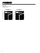
CM400DU-24H
Dual IGBTMOD™ U-Series Module
400 Amperes/1200 Volts
Powerex, Inc., 200 Hillis Street, Youngwood, Pennsylvania 15697-1800 (724) 925-7272
Absolute Maximum Ratings, T
j
= 25 °C unless otherwise specified
Ratings Symbol CM400DU-24H Units
Junction Temperature T
j
-40 to 150 °C
Storage Temperature T
stg
-40 to 125 °C
Collector-Emitter Voltage (G-E SHORT) V
CES
1200 Volts
Gate-Emitter Voltage (C-E SHORT) V
GES
±20 Volts
Collector Current (T
c
= 25°C) I
C
400 Amperes
Peak Collector Current I
CM
800* Amperes
Emitter Current** (T
c
= 25°C) I
E
400 Amperes
Peak Emitter Current** I
EM
800* Amperes
Maximum Collector Dissipation (T
c
= 25°C, T
j
≤ 150°C) P
c
2100 Watts
Mounting Torque, M8 Main Terminal – 95 in-lb
Mounting Torque, M6 Mounting – 40 in-lb
G(E) Terminal, M4 – 15 in-lb
Weight – 310 Grams
Isolation Voltage (Main Terminal to Baseplate, AC 1 min.) V
iso
2500 Volts
* Pulse width and repetition rate should be such that the device junction temperature (T
j
) does not exceed T
j(max)
rating.
**Represents characteristics of the anti-parallel, emitter-to-collector free-wheel diode (FWDi).
Static Electrical Characteristics, T
j
= 25 °C unless otherwise specified
Characteristics Symbol Test Conditions Min. Typ. Max. Units
Collector-Cutoff Current I
CES
V
CE
= V
CES
, V
GE
= 0V ––2mA
Gate Leakage Voltage I
GES
V
GE
= V
CES
, V
CE
= 0V ––0.5 µA
Gate-Emitter Threshold Voltage V
GE(th)
I
C
= 40mA, V
CE
= 10V 4.5 6 7.5 Volts
Collector-Emitter Saturation Voltage V
CE(sat)
I
C
= 400A, V
GE
= 15V, T
j
= 25°C – 2.9 3.7 Volts
I
C
= 400A, V
GE
= 15V, T
j
= 125°C – 2.85 – Volts
Total Gate Charge Q
G
V
CC
= 600V, I
C
= 400A, V
GE
= 15V – 1500 – nC
Emitter-Collector Voltage** V
EC
I
E
= 400A, V
GE
= 0V ––3.2 Volts
**Represents characteristics of the anti-parallel, emitter-to-collector free-wheel diode (FWDi).
Dynamic Electrical Characteristics, T
j
= 25 °C unless otherwise specified
Characteristics Symbol Test Conditions Min. Typ. Max. Units
Input Capacitance C
ies
––60 nf
Output Capacitance C
oes
V
CE
= 10V, V
GE
= 0V ––21 nf
Reverse Transfer Capacitance C
res
––12 nf
Resistive Turn-on Delay Time t
d(on)
V
CC
= 600V, I
C
= 400A, –––ns
Load Rise Time t
r
V
GE1
= V
GE2
= 15V, –––ns
Switch Turn-off Delay Time t
d(off)
R
G
= 0.78⍀, Resistive –––ns
Times Fall Time t
f
Load Switching Operation –––ns
Diode Reverse Recovery Time** t
rr
I
E
= 400A, di
E
/dt = -800A/µs ––300 ns
Diode Reverse Recovery Charge** Q
rr
I
E
= 400A, di
E
/dt = -800A/µs – 2.2 – µC
**Represents characteristics of the anti-parallel, emitter-to-collector free-wheel diode (FWDi).
Thermal and Mechanical Characteristics, T
j
= 25 °C unless otherwise specified
Characteristics Symbol Test Conditions Min. Typ. Max. Units
Thermal Resistance, Junction to Case R
th(j-c)
Q Per IGBT 1/2 Module ––0.06 °C/W
Thermal Resistance, Junction to Case R
th(j-c)
R Per FWDi 1/2 Module ––0.09 °C/W
Contact Thermal Resistance R
th(c-f)
Per Module, Thermal Grease Applied – 0.019 – °C/W
2