
Instruction Manual

CM200TL-12NF
Six IGBTMOD™ NF-Series Module
200 Amperes/600 Volts
2
Powerex, Inc., 200 E. Hillis Street, Youngwood, Pennsylvania 15697-1800 (724) 925-7272
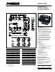
Absolute Maximum Ratings, T
j
= 25°C unless otherwise specified
Characteristics Symbol CM200TL-12NF Units
Power Device Junction Temperature T
j
-40 to 150 °C
Storage Temperature T
stg
-40 to 125 °C
Collector-Emitter Voltage (G-E Short) V
CES
600 Volts
Gate-Emitter Voltage (C-E Short) V
GES
±20 Volts
Collector Current (T
C
= 88°C)* I
C
200 Amperes
Peak Collector Current (Tj ≤ 150°C) I
CM
400** Amperes
Emitter Current*** I
E
200 Amperes
Peak Emitter Current*** I
EM
400** Amperes
Maximum Collector Dissipation (T
C
= 25°C, T
j
< 150°C) P
C
890 Watts
Mounting Torque, M5 Mounting Screws — 31 in-lb
Mounting Torque, M5 Main Terminal Screws — 31 in-lb
Module Weight (Typical) — 750 Grams
Isolation Voltage, AC 1 minute, 60Hz Sinusoidal V
ISO
2500 Volts
Electrical and Mechanical Characteristics, T
j
= 25°C unless otherwise specified
Characteristics Symbol Test Conditions Min. Typ. Max. Units
Collector Cutoff Current I
CES
V
CE
= V
CES
, V
GE
= 0V — — 1.0 mA
Gate-Emitter Threshold Voltage V
GE(th)
I
C
= 20mA, V
CE
= 10V 6 7 8 Volts
Gate Leakage Current I
GES
V
GE
= V
GES
, V
CE
= 0V — — 0.5 µA
Collector-Emitter Saturation Voltage V
CE(sat)
I
C
= 200A, V
GE
= 15V, T
j
= 25°C — 1.7 2.2 Volts
I
C
= 200A, V
GE
= 15V, T
j
= 125°C — 1.7 — Volts
Input Capacitance C
ies
— — 30.0 nf
Output Capacitance C
oes
V
CE
= 10V, V
GE
= 0V — — 3.7 nf
Reverse Transfer Capacitance C
res
— — 1.2 nf
Total Gate Charge Q
G
V
CC
= 300V, I
C
= 200A, V
GE
= 15V — 800 — nC
Inductive Turn-on Delay Time t
d(on)
— — 120 ns
Load Turn-on Rise Time t
r
V
CC
= 300V, I
C
= 200A, — — 100 ns
Switch Turn-off Delay Time t
d(off)
V
GE1
= V
GE2
= 15V, — — 300 ns
Time Turn-off Fall Time t
f
R
G
= 3.1Ω, I
E
= 200A, — — 300 ns
Reverse Recovery Time*** t
rr
Inductive Load Switching Operation — — 150 ns
Reverse Recovery Charge*** Qrr — 4.8 — µC
Emitter-Collector Voltage*** V
EC
I
E
= 200A, V
GE
= 0V — — 2.8 Volts
*T
C
, T
f
measured point is just under the chips.
**Pulse width and repetition rate should be such that device junction temperature (T
j
) does not exceed T
j(max)
rating.
***Represents characteristics of the anti-parallel, emitter-to-collector free-wheel diode (FWDi).