
User Manual

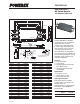

CM150DX-24A
Dual IGBTMOD™ NX-Series Module
150 Amperes/1200 Volts
Powerex, Inc., 173 Pavilion Lane, Youngwood, Pennsylvania 15697 (724) 925-7272
3Rev. 3/09
Electrical and Mechanical Characteristics, T
j
= 25°C unless otherwise specied
Inverter Sector
Characteristics Symbol Test Conditions Min. Typ. Max. Units
Collector Cutoff Current I
CES
V
CE
= V
CES
, V
GE
= 0V — — 1.0 mA
Gate-Emitter Threshold Voltage V
GE(th)
I
C
= 15mA, V
CE
= 10V 6 7 8 Volts
Gate Leakage Current I
GES
V
GE
= V
GES
, V
CE
= 0V — — 0.5 µA
Collector-Emitter Saturation Voltage V
CE(sat)
I
C
= 150A, V
GE
= 15V, T
j
= 25°C
*5
— 2.0 2.6 Volts
I
C
= 150A, V
GE
= 15V, T
j
= 125°C
*5
— 2.2 — Volts
I
C
= 150A, V
GE
= 15V, Chip — 1.9 — Volts
Input Capacitance C
ies
— — 23.0 nF
Output Capacitance C
oes
V
CE
= 10V, V
GE
= 0V — — 2.0 nF
Reverse Transfer Capacitance C
res
— — 0.45 nF
Total Gate Charge Q
G
V
CC
= 600V, I
C
= 150A, V
GE
= 15V — 675 — nC
Inductive Turn-on Delay Time t
d(on)
— — 130 ns
Load Turn-on Rise Time t
r
V
CC
= 600V, I
C
= 150A, — — 100 ns
Switch Turn-off Delay Time t
d(off)
V
GE
= ±15V, — — 450 ns
Time Turn-off Fall Time t
f
R
G
= 2.2Ω, I
E
= 150A, — — 600 ns
Reverse Recovery Time t
rr
*2
Inductive Load Switching Operation — — 150 ns
Reverse Recovery Charge Qrr
*2
— 6 — µC
Emitter-Collector Voltage V
EC
*2
I
E
= 150A, V
GE
= 0V, T
j
= 25°C
*5
— 2.6 3.4 Volts
I
E
= 150A, V
GE
= 0V, T
j
= 125°C
*5
— 2.16 — Volts
I
E
= 150A, V
GE
= 0V, Chip — 2.5 — Volts
Thermal and Mechanical Characteristics, T
j
= 25°C unless otherwise specied
Characteristics Symbol Test Conditions Min. Typ. Max. Units
Module Lead Resistance R
lead
Main Termnals-Chip (Per Switch) — 1.6 — mΩ
Thermal Resistance, Junction to Case** R
th(j-c)
Q Per IGBT
*1
— — 0.13 °C/W
Thermal Resistance, Junction to Case** R
th(j-c)
D Per FWDi
*1
— — 0.23 °C/W
Contact Thermal Resistance** R
th(c-f)
Case to Heatsink (Per 1 Module) — 0.015 — °C/W
Thermal Grease Applied
*1*7
Internal Gate Resistance R
Gint
T
C
= 25°C — 0 — Ω
External Gate Resistance R
G
2 — 21 Ω
NTC Thermistor Sector, T
j
= 25°C unless otherwise specied
Characteristics Symbol Test Conditions Min. Typ. Max. Units
Zero Power Resistance R
TH
T
C
= 25°C
*1
4.85 5.00 5.15 kΩ
Deviation of Resistance ∆R/R T
C
= 100°C, R
100
= 493Ω
*1
–7.3 — +7.8 %
B Constant B
(25/50)
B = (InR
1
– InR
2
) / (1/T
1
– 1/T
2
)
*6
— 3375 — K
Power Dissipation P
25
T
C
= 25°C
*1
— — 10 mW
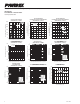
**Thermal resistance values are per 1 element.
*1 Case temperature (T
C
) and heatsink temperature (T
f
) are defined on the surface of the baseplate and heatsink at just under the chip.
*2 I
E
, I
EM
, V
EC
, t
rr
and Q
rr
represent ratings and characteristics of the anti-parallel, emitter-to-collector free-wheel diode (FWDi).
*5 Pulse width and repetition rate should be such as to cause negligible temperature rise.
*6 R
1
: Resistance at Absolute Temperature T
1
(K), R
2
: Resistance at Absolute Temperature T
2
(K), T(K) = T(°C) + 273.15
*7 Typical value is measured by using thermally conductive grease of λ = 0.9 [W/(m • K)].