
Instruction Manual

CM1400E3U-24NF
Mega Power Chopper IGBTMOD™
1400 Amperes/1200 Volts
3
Powerex, Inc., 173 Pavilion Lane, Youngwood, Pennsylvania 15697 (724) 925-7272
09/08
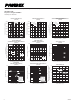
Electrical Characteristics, T
j
= 25°C unless otherwise specied
Characteristics Symbol Test Conditions Min. Typ. Max. Units
Collector-Cutoff Current I
CES
V
CE
= V
CES
, V
GE
= 0V – – 1 mA
Gate-Emitter Threshold Voltage V
GE(th)
I
C
= 140mA, V
CE
= 10V 6 7 8 Volts
Gate Leakage Current I
GES
V
GE
= V
GES
, V
CE
= 0V – – 1.5 μA
Collector-Emitter Saturation Voltage V
CE(sat)
I
C
= 1400A, V
GE
= 15V, T
j
= 25°C – 1.8 2.5 Volts
(Without Lead Resistance) (Chip) I
C
= 1400A, V
GE
= 15V, T
j
= 125°C – 2.0 – Volts
Module Lead Resistance R
(lead)
I
C
= 1400A, Terminal-Chip – 0.286 – mΩ
Input Capacitance C
ies
– – 220 nF
Output Capacitance C
oes
V
CE
= 10V, V
GE
= 0V – – 25 nF
Reverse Transfer Capacitance C
res
– – 4.7 nF
Total Gate Charge Q
G
V
CC
= 600V, I
C
= 1400A, V
GE
= 15V – 7200 – nC
Inductive Turn-on Delay Time t
d(on)
V
CC
= 600V, I
C
= 1400A, – – 800 ns
Load Rise Time t
r
V
GE1
= V
GE2
= 15V, – – 300 ns
Switch Turn-off Delay Time t
d(off)
R
G
= 0.22Ω, Inductive Load – – 1000 ns
Times Fall Time t
f
Switching Operation – – 300 ns
Reverse Recovery Time* t
rr
I
E
= 100A – – 700 ns
Reverse Recovery Charge* Q
rr
– 90 – μC
Emitter-Collector Voltage** V
EC
I
E
= 100A, V
GE
= 0V – – 3.0 Volts
External Gate Resistance R
G
0.22 – 2.2 Ω
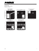
Clamp Diode Characteristics, T
j
= 25°C unless otherwise specied
Characteristics Symbol Test Conditions Min. Typ. Max. Units
Emitter-Collector Voltage V
FM
I
F
=1400A, Clamp Diode Part – – 3.2 Volts
(without Lead Resistance) (Chip)
Reverse Recovery Time t
rr
I
F
=1400A, Clamp Diode Part – – 700 ns
Reverse Recovery Charge Q
rr
– 90 – μC
* Pulse width and repetition rate should be such that the device junction temperature (T
j
) does not exceed T
j(max)
rating.
** Represents characteristics of the anti-parallel, emitter-to-collector free-wheel diode (FWDi).
Thermal and Mechanical Characteristics, T
j
= 25°C unless otherwise specied
Characteristics Symbol Test Conditions Min. Typ. Max. Units
Thermal Resistance, Junction to Case R
th(j-c)
Q Per IGBT 1/2 Module, T
C
Reference – – 0.032 °C/W
Point per Outline Drawing
Thermal Resistance, Junction to Case R
th(j-c)
D Per Clamp Diode 1/2 Module, – – 0.053 °C/W
T
C
Reference Point per Outline Drawing
Thermal Resistance, Junction to Case R
th(j-c')
Q Per IGBT 1/2 Module, – – 0.014 °C/W
T
C
Reference Point Under Chip
Thermal Resistance, Junction to Case R
th(j-c')
D Per Clamp Diode 1/2 Module, – – 0.023 °C/W
T
C
Reference Point Under Chip
Contact Thermal Resistance R
th(c-f)
Per 1/2 Module, Thermal Grease Applied – 0.016 – °C/W