
Owner manual

CM1400DU-24NF
Mega Power Dual IGBTMOD™
1400 Amperes/1200 Volts
2
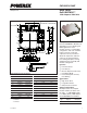
Powerex, Inc., 173 Pavilion Lane, Youngwood, Pennsylvania 15697 (724) 925-7272 www.pwrx.com
11/11 Rev. 2
Maximum Ratings, T
j
= 25°C unless otherwise specied
Ratings Symbol Ratings Units
Collector-Emitter Voltage (G-E SHORT) V
CES
1200 Volts
Gate-Emitter Voltage (C-E SHORT) V
GES
±20 Volts
Collector Current DC (T
C'
= 94°C)
*5
I
C
1400 Amperes
Peak Collector Current (Pulse)
*2
I
CM
2800 Amperes
Emitter Current (T
C
= 25°C) I
E
*1
1400 Amperes
Peak Emitter Current (Pulse)
*2
I
EM
*1
2800 Amperes
Maximum Collector Dissipation (T
C
= 25°C) P
C
*3
3900 Watts
Junction Temperature T
j
-40 to 150 °C
Storage Temperature
*4
T
stg
-40 to 125 °C
Isolation Voltage (Terminals to Baseplate, f = 60Hz, AC 1 min.) V
iso
2500 Volts
Mounting Torque, M6 Mounting Screws – 40 in-lb
Mounting Torque, M6 Main Terminal Screw – 40 in-lb
Weight (Typical) – 1400 Grams
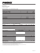
Electrical Characteristics, T
j
= 25°C unless otherwise specied
Characteristics Symbol Test Conditions Min. Typ. Max. Units
Collector-Cutoff Current I
CES
V
CE
= V
CES
, V
GE
= 0V – – 1 mA
Gate-Emitter Threshold Voltage V
GE(th)
I
C
= 140mA, V
CE
= 10V 6 7 8 Volts
Gate Leakage Current I
GES
±V
GE
= V
GES
, V
CE
= 0V – – 1.5 μA
Collector-Emitter Saturation Voltage V
CE(sat)
I
C
= 1400A, V
GE
= 15V, T
j
= 25°C
*4
– 1.8 2.5 Volts
(Without Lead Resistance) (Chip) I
C
= 1400A, V
GE
= 15V, T
j
= 125°C
*4
– 2.0 – Volts
Module Lead Resistance R
(lead)
I
C
= 1400A, Terminal-Chip – 0.286 – mΩ
Input Capacitance C
ies
– – 220 nF
Output Capacitance C
oes
V
CE
= 10V, V
GE
= 0V – – 25 nF
Reverse Transfer Capacitance C
res
– – 4.7 nF
Total Gate Charge Q
G
V
CC
= 600V, I
C
= 1400A, V
GE
= 15V – 7200 – nC
Turn-on Delay Time t
d(on)
– – 800 ns
Turn-on Rise Time t
r
V
CC
= 600V, I
C
= 1400A, – – 300 ns
Turn-off Delay Time t
d(off)
V
GE
= ±15V, – – 1000 ns
Turn-off Fall Time t
f
R
G
= 0.22Ω, Inductive Load, – – 300 ns
Reverse Recovery Time t
rr
*1
I
E
= 1400A – – 700 ns
Reverse Recovery Charge Q
rr
*1
– 90 – µC
Emitter-Collector Voltage V
EC
*1
I
E
= 1400A, V
GE
= 0V – – 3.2 Volts
(Without Lead Resistance) (Chip)
*1 Represent ratings and characteristics of the anti-parallel, emitter-to-collector free wheeling diode (FWDi).
*2 Pulse width and repetition rate should be such that device junction temperature (T
j
) does not exceed T
j(max)
rating.
*3 Junction temperature (T
j
) should not increase beyond maximum junction temperature (T
j(max)
) rating.
*4 Pulse width and repetition rate should be such as to cause negligible temperature rise.
*5 Case temperature (T
C
') measured point is just under the chips. If you use this value, Rth(f-a) should be measured just under the chips.
*8 The operation temperature is restrained by the permission temperature of female connector.