
Owner manual

Jul. 2005
MITSUBISHI HVIGBT MODULES
CM1200HG-66H
HIGH POWER SWITCHING USE
INSULATED TYPE
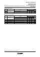
V
V
V
CE = VCES, VGE = 0V, Tj = 25°C
V
GE = VGES, VCE = 0V, Tj = 25°C
I
C = 1200A, VGE = 15V, Tj = 25°C (Note 4)
I
C = 1200A, VGE = 15V, Tj = 125°C (Note 4)
V
CC = 1650V, IC = 1200A, VGE = 15V, Tj = 25°C
I
E = 1200A, VGE = 0V, Tj = 25°C (Note 4)
I
E = 1200A, VGE = 0V, Tj = 125°C (Note 4)
V
CC = 1650V, IC = 1200A, VGE = ±15V
R
G(on) = 1.6Ω, Tj = 125°C, Ls = 100nH
Inductive load
V
CC = 1650V, IC = 1200A, VGE = ±15V
R
G(off) = 1.6Ω, Tj = 125°C, Ls = 100nH
Inductive load
V
CC = 1650V, IC = 1200A, VGE = ±15V
R
G(on) = 1.6Ω, Tj = 125°C, Ls = 100nH
Inductive load
I
C = 120mA, VCE = 10V, Tj = 25°C
V
CE = 10V, f = 100kHz
V
GE = 0V, Tj = 25°C
Collector cut-off current
Gate-emitter
threshold voltage
Gate leakage current
Collector-emitter
saturation voltage
Input capacitance
Output capacitance
Reverse transfer capacitance
Total gate charge
Emitter-collector voltage
Turn-on delay time
Turn-on rise time
Turn-on switching energy
Turn-off delay time
Turn-off fall time
Turn-off switching energy
Reverse recovery time
Reverse recovery charge
Reverse recovery energy
Collector-emitter voltage
Gate-emitter voltage
Maximum power dissipation
Junction temperature
Operating temperature
Storage temperature
Isolation voltage
Partial discharge
Maximum short circuit pulse
width
VGE = 0V, Tj = 25°C
V
CE = 0V, Tj = 25°C
T
C = 90°C
Pulse (Note 1)
Pulse (Note 1)
T
C = 25°C, IGBT part
RMS, sinusoidal, f = 60Hz, t = 1min.
V1 = 6900V
rms, V2 = 5100Vrms
f = 60Hz (acc. to IEC 1287)
V
CC = 2200V, VCES ≤ 3300V, VGE = 15V
T
j = 125°C
Collector current
Emitter current
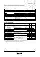
3300
±20
1200
2400
1200
2400
12500
–40 ~ +150
–40 ~ +125
–40 ~ +125
10200
10
10
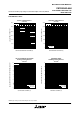
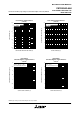
MAXIMUM RATINGS
Symbol Item Conditions UnitRatings
V
V
A
A
A
A
W
°C
°C
°C
V
pC
µs
V
CES
VGES
IC
ICM
IE
(Note 2)
IEM
(Note 2)
PC
(Note 3)
Tj
Top
Tstg
Viso
Qpd
tpsc
Min Typ Max
15
0.5
4.20
—
—
—
—
—
3.60
—
1.60
1.00
—
2.50
1.00
—
1.40
—
—
mA
µA
nF
nF
nF
µC
V
µs
µs
J/pulse
µs
µs
J/pulse
µs
µC
J/pulse
—
—
3.30
3.60
180
18.0
5.4
8.6
2.80
2.70
—
—
1.60
—
—
1.55
—
800
0.90
—
—
—
—
—
—
—
—
—
—
—
—
—
—
—
—
—
—
—
I
CES
IGES
Cies
Coes
Cres
Qg
VEC
(Note 2)
td(on)
tr
Eon
td(off)
tf
Eoff
trr
(Note 2)
Qrr
(Note 2)
Erec
(Note 2)
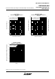
ELECTRICAL CHARACTERISTICS
Symbol
Item Conditions
V
GE(th)
VCE(sat)
Limits
Unit
6.0
5.0
Note 1. Pulse width and repetition rate should be such that junction temperature (Tj) does not exceed Topmax rating (125°C).
2. The symbols represent characteristics of the anti-parallel, emitter to collector free-wheel diode (FWDi).
3. Junction temperature (T
j) should not exceed Tjmax rating (150°C).
4. Pulse width and repetition rate should be such as to cause negligible temperature rise.
7.0
3rd-Version HVIGBT (High Voltage Insulated Gate Bipolar Transistor) Modules
HVIGBT (High Voltage Insulated Gate Bipolar Transistor) Modules