
Owner's manual

CM100TX-24S
Six IGBTMOD™ NX-S Series Module
100 Amperes/1200 Volts
Powerex, Inc., 173 Pavilion Lane, Youngwood, Pennsylvania 15697 (724) 925-7272 www.pwrx.com
307/11 Rev. 2
Electrical Characteristics, T
j
= 25°C unless otherwise specied
Inverter Part IGBT/FWDi
Characteristics Symbol Test Conditions Min. Typ. Max. Units
Collector-Emitter Cutoff Current I
CES
V
CE
= V
CES
, V
GE
= 0V — — 1 mA
Gate-Emitter Leakage Current I
GES
V
GE
= V
GES
, V
CE
= 0V — — 0.5 µA
Gate-Emitter Threshold Voltage V
GE(th)
I
C
= 10mA, V
CE
= 10V 5.4 6.0 6.6 Volts
Collector-Emitter Saturation Voltage V
CE(sat)
I
C
= 100A, V
GE
= 15V, T
j
= 25°C
*5
— 1.80 2.25 Volts
(Terminal) I
C
= 100A, V
GE
= 15V, T
j
= 125°C
*5
— 2.00 — Volts
I
C
= 100A, V
GE
= 15V, T
j
= 150°C
*5
— 2.05 — Volts
Collector-Emitter Saturation Voltage V
CE(sat)
I
C
= 100A, V
GE
= 15V, T
j
= 25°C
*5
— 1.70 2.15 Volts
(Chip) I
C
= 100A, V
GE
= 15V, T
j
= 125°C
*5
— 1.90 — Volts
I
C
= 100A, V
GE
= 15V, T
j
= 150°C
*5
— 1.95 — Volts
Input Capacitance C
ies
— — 10 nF
Output Capacitance C
oes
V
CE
= 10V, V
GE
= 0V — — 2.0 nF
Reverse Transfer Capacitance C
res
— — 0.17 nF
Gate Charge Q
G
V
CC
= 600V, I
C
= 100A, V
GE
= 15V — 233 — nC
Turn-on Delay Time t
d(on)
— — 300 ns
Rise Time t
r
V
CC
= 600V, I
C
= 100A, V
GE
= ±15V, — — 200 ns
Turn-off Delay Time t
d(off)
R
G
= 6.2Ω, Inductive Load — — 600 ns
Fall Time t
f
— — 300 ns
Emitter-Collector Voltage V
EC
*1
I
E
= 100A, V
GE
= 0V, T
j
= 25°C
*5
— 1.80 2.25 Volts
(Terminal) I
E
= 100A, V
GE
= 0V, T
j
= 125°C
*5
— 1.80 — Volts
I
E
= 100A, V
GE
= 0V, T
j
= 150°C
*5
— 1.80 — Volts
Emitter-Collector Voltage V
EC
*1
I
E
= 100A, V
GE
= 0V, T
j
= 25°C
*5
— 1.70 2.15 Volts
(Chip) I
E
= 100A, V
GE
= 0V, T
j
= 125°C
*5
— 1.70 — Volts
I
E
= 100A, V
GE
= 0V, T
j
= 150°C
*5
— 1.70 — Volts
Reverse Recovery Time t
rr
*1
V
CC
= 600V, I
E
= 100A, V
GE
= ±15V — — 300 ns
Reverse Recovery Charge Q
rr
*1
R
G
= 6.2Ω, Inductive Load — 5.3 — µC
Turn-on switching Energy per Pulse E
on
V
CC
= 600V, I
C
= I
E
= 100A, V
GE
= ±15V — 8.6 — mJ
Turn-off switching Energy per Pulse E
off
R
G
= 6.2Ω, T
j
= 150°C — 10.7 — mJ
Reverse Recovery Energy per Pulse E
rr
*1
Inductive Load — 10.2 — mJ
Internal Lead Resistance R
CC' + EE'
Main Terminals-Chip, — — 2.2 mΩ
Per Switch,T
C
= 25°C
*2
Internal Gate Resistance r
g
Per Switch — 0 — Ω
*1 Represent ratings and characteristics of the anti-parallel, emitter-to-collector free wheeling
diode (FWDi).
*2 Case temperature (T
C
) and heatsink temperature (T
s
) is measured on the surface
(mounting side) of the baseplate and the heatsink side just under the chips.
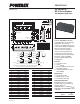
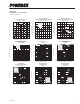
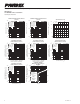
Refer to the figure to the right for chip location.
The heatsink thermal resistance should be measured just under the chips.
*5 Pulse width and repetition rate should be such as to cause negligible temperature rise.
1 2 3 4 5 6 7 8 9 10 11 12 13 14 15 16 17 18 19 20 21 22
53
54
55
56
57
58
59
60
61
30
29
28
27
26
25
24
23
52 51 50 49 48 47 46 45 44 43 42 41 40 39 38 37 36 35 34 33 32 31
0 0
20.2
29.5
LABEL SIDE
Each mark points to the center position of each chip.
Tr*P / Tr*N: IGBT Di*P / Di*N: FWDi Th: NTC Thermistor
20.6
0
33.7
51.6
64.7
82.6
95.7
24.1
104.5
Di
UP
Di
VP
Di
WP
Tr
UP
Tr
VP
Tr
WP
Di
UN
Di
VN
Di
WN
Tr
UN
Tr
VN
Tr
WN
Th