
User Manual

CM100RX-24S
Six IGBTMOD™ + Brake NX-S Series Module
100 Amperes/1200 Volts
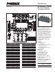
Powerex, Inc., 173 Pavilion Lane, Youngwood, Pennsylvania 15697 (724) 925-7272 www.pwrx.com
506/11 Rev. 2
Electrical Characteristics, T
j
= 25°C unless otherwise specied
NTC Thermistor Part
Characteristics Symbol Test Conditions Min. Typ. Max. Units
Zero Power Resistance R
25
T
C
= 25°C
*2
4.85 5.00 5.15 kΩ
Deviation of Resistance ∆R/R T
C
= 100°C
*2
, R
100
= 493Ω -7.3 — +7.8 %
B Constant B
(25/50)
Approximate by Equation
*6
— 3375 — K
Power Dissipation P
25
T
C
= 25°C
*2
— — 10 mW
Thermal Resistance Characteristics, T
j
= 25°C unless otherwise specied
Thermal Resistance, Junction to Case
*2
R
th(j-c)
Q Per Inverter IGBT — — 0.20 K/W
Thermal Resistance, Junction to Case
*2
R
th(j-c)
D Per Inverter FWDi — — 0.29 K/W
Thermal Resistance, Junction to Case
*2
R
th(j-c)
Q Per Brake IGBT — — 0.35 K/W
Thermal Resistance, Junction to Case
*2
R
th(j-c)
D Brake Part ClampDi — — 0.63 K/W
Contact Thermal Resistance, R
th(c-s)
Thermal Grease Applied, — 0.015 — K/W
Case to Heatsink
*2
per 1 Module
*7
Mechanical Characteristics
Mounting Torque M
t
Main Terminals, M5 Screw 22 27 31 in-lb
Mounting Torque M
s
Mounting to Heatsink, M5 Screw 22 27 31 in-lb
Creepage Distance d
s
Terminal to Terminal 10.25 — — mm
Terminal to Baseplate 12.32 — — mm
Clearance d
a
Terminal to Terminal 10.28 — — mm
Terminal to Baseplate 10.85 — — mm
Weight m — 370 — Grams
Flatness of Baseplate e
c
On Centerline X, Y
*8
±0 — ±100 µm
Recommended Operating Conditons, T
a
= 25°C
(DC) Supply Voltage V
CC
Applied Across P-N/P1-N1 Terminals — 600 850 Volts
Gate (-Emitter Drive) Voltage V
GE(on)
Applied Across GB-EsB / G*P-Es*P/ 13.5 15.0 16.5 Volts
G*N-Es*N (* = U, V, W) Terminals
External Gate Resistance R
G
Per Switch, Inverter IGBT 8.2 — 82 Ω
Per Switch, Brake IGBT 13 — 130 Ω
*2 Case temperature (T
C
) and heatsink temperature (T
s
) is measured on the surface (mounting side) of the baseplate and the heatsink side just under the chips.
Refer to the figure on page 1 for chip location. The heatsink thermal resistance should be measured just under the chips.
*5 Pulse width and repetition rate should be such as to cause negligible temperature rise.
*6 B
(25/50)
= In(
R
25
)/(
1
–
1
)
R
50
T
25
T
50
R
25
; Resistance at Absolute Temperature T
25
[K]; T
25
= 25 [°C] + 273.15 = 298.15 [K]
R
50
; Resistance at Absolute Temperature T
50
[K]; T
50
= 50 [°C] + 273.15 = 323.15 [K]
*7 Typical value is measured by using thermally conductive grease of λ = 0.9 [W/(m • K)].
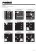
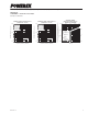
*8 Baseplate (mounting side) flatness measurement points (X, Y) are shown in the figure.
– : CONCAVE
+ : CONVEX
– : CONCAVE
X
Y
+ : CONVEX
MOUNTING
SIDE
MOUNTING SIDE
MOUNTING SIDE