6121 Baker Road, Suite 108 Minnetonka, MN 55345 Phone (952) 933-6190 Fax (952) 933-6223 1-800-274-4284 www.chtechnology.com Thank you for downloading this document from C&H Technology, Inc. Please contact the C&H Technology team for the following questions - Technical Application Assembly Availability Pricing Phone – 1-800-274-4284 E-Mail – sales@chtechnology.com www.chtechnology.com - SPECIALISTS IN POWER ELECTRONIC COMPONENTS AND ASSEMBLIES - www.chtechnology.
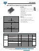
70MT060WSP www.vishay.com Vishay Semiconductors MTP IGBT Power Module Primary Rectifier and PFC FEATURES • Input rectifier bridge • PFC stage with warp 2 IGBT and FRED Pt® hyperfast diode • Very low stray inductance design for high speed operation • Integrated thermistor • Isolated baseplate MTP • Compliant to RoHS Directive 2002/95/EC • Designed and qualified for industrial level PRODUCT SUMMARY BENEFITS INPUT BRIDGE DIODE, TJ = 150 °C VRRM 1200 V lO at 80 °C 48 A VFM at 25 °C at 20 A 1.
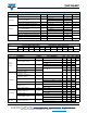
70MT060WSP www.vishay.com Vishay Semiconductors ABSOLUTE MAXIMUM RATINGS PARAMETER SYMBOL Repetitive peak reverse voltage IF UNITS 600 V TC = 25 °C 82 TC = 80 °C 55 A PD TC = 25 °C 181 W Maximum non-repetitive peak current IFSM TC = 25 °C 360 A Repetitive peak reverse voltage VRRM 600 V Maximum power dissipation TC = 25 °C 21 TC = 80 °C 13 PD TC = 25 °C 32 W IFSM TC = 25 °C 60 A Maximum continuous forward current TJ = 150 °C maximum AP Diode MAX.
70MT060WSP www.vishay.com Vishay Semiconductors ELECTRICAL SPECIFICATIONS (TJ = 25 °C unless otherwise noted) PARAMETER SYMBOL TEST CONDITIONS MIN. TYP. MAX.
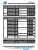
70MT060WSP www.vishay.com Vishay Semiconductors THERMAL AND MECHANICAL SPECIFICATIONS PARAMETER Input Rectifier Bridge SYMBOL MIN. TYP. MAX. - - 0.9 Junction to case diode thermal resistance PFC IGBT Junction to case IGBT thermal resistance PFC Diode Junction to case PFC diode thermal resistance AP Diode Junction to case AP diode thermal resistance RthJC Case to sink, flat, greased surface per module Mounting torque ± 10 % to heatsink RthCS (1) Approximate weight UNITS - - 0.
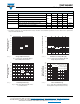
70MT060WSP ZthJC - Thermal Impedance (°C/W) www.vishay.com Vishay Semiconductors 10 Steady state value RthJC = 0.9 °C/W (DC operation) 1 0.1 0.01 0.00001 0.0001 0.001 0.01 0.1 1 10 t1 - Rectangular Pulse Duration (s) 93410_05 250 160 140 200 VGE = 18 V 120 100 IC (A) Allowable Case Temperature (°C) Fig.
0MT060WSP www.vishay.com 250 IC (A) 200 150 TC = 125 °C 100 TC = 25 °C 50 0 3 4 5 6 7 8 VGE (V) 93410_10 IF - Instantaneous Forward Current (A) Vishay Semiconductors 90 80 70 50 TC = 125 °C ICES (mA) 0.1 0.01 TC = 25 °C 30 20 TJ = 25 °C 10 0 0.5 1.0 1.5 2.0 2.5 3.0 160 140 120 100 80 60 40 20 0 200 300 400 500 600 VCES (V) 93410_11 0 4.0 TC = 25 °C 3.5 3.0 TC = 125 °C 2.5 2.0 0.3 0.4 0.5 0.6 0.7 0.8 0.9 Fig.
70MT060WSP Vishay Semiconductors 1.6 160 140 1.2 120 Energy (mJ) Allowable Case Temperature (°C) www.vishay.com 100 80 60 0.8 Eoff Eon 0.4 40 20 0 0 0 20 40 60 80 IF - Continuous Forward Current (A) 93410_16 0 100 10 20 Fig. 16 - Maximum Continuous Forward Current vs. Case Temperature PFC Diode 40 50 Fig. 19 - Typical IGBT Energy Loss vs. Rg TJ = 125 °C, IC = 70 A, VCC = 360 V, VGE = 15 V, L = 500 μH, Rg = 5 1 Switching Time (ns) 1000 TJ = 150 °C IR (mA) 0.1 0.
70MT060WSP www.vishay.com Vishay Semiconductors 150 150 trr (ns) trr (ns) TJ = 125 °C TJ = 125 °C 100 100 TJ = 25 °C 50 100 TJ = 25 °C 200 300 400 dIF/dt (A/μs) 93410_22 50 100 500 200 Fig. 22 - Typical trr Antiparallel Diode vs. dIF/dt Vrr = 200 V, IF = 4 A 300 400 500 dIF/dt (A/μs) 93410_25 Fig. 25 - Typical trr Chopper Diode vs.
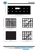
70MT060WSP ZthJC - Transient Thermal Impedance Junction to Case (°C/W) www.vishay.com Vishay Semiconductors 1 0.1 D = 0.50 D = 0.20 D = 0.10 D = 0.05 D = 0.02 D = 0.01 DC 0.01 0.0001 0.001 0.01 0.1 1 10 t1 - Rectangular Pulse Duration (s) 93410_28 Fig. 28 - Maximum Thermal Impedance ZthJC Characteristics (IGBT) Driver L D.U.T. 0 + VCC - D + C - 1K 900 V D.U.T. Fig. C.T.1 - Gate Charge Circuit (Turn-Off) Fig. C.T.3 - S.C. SOA Circuit L Diode clamp/ D.U.T. + - 80 V L + - D.U.T.
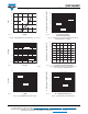
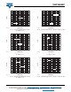
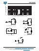
70MT060WSP www.vishay.com Vishay Semiconductors CIRCUIT CONFIGURATION G1 H1 A1 B1 D1 D3 E7 D6 Th M1 M3 A4 F7 Q1 C4 D5 H7 D2 D4 M7 D1 E1 A7 C7 DIMENSIONS in millimeters 12.1 ± 0.3 Ø 1.1 ± 0.025 2.1 1.5 3.0 39.5 ± 0.3 12 ± 0.3 17± 0.3 3 2.5 ± 0.1 6 z detail Use Self Tapping Screw or M2.5 x X. e.g. M2.5 x 6 or M2.5 x 8 according to Pcb thickness used 45 ± 0.1 63.5 ± 0.15 0.8 Ra 48.7 ± 0.3 1.3 21.1 ± 0.5 7.4 4.1 A B C D E F G H I L M X 7 6 Ø 2.1(X4) 12 27.5 ± 0.3 Diam.
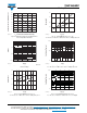
Outline Dimensions Vishay Semiconductors MTP - Full Pin DIMENSIONS in millimeters 3.0 2.1 1.5 z detail 12 ± 0.3 39.5 ± 0.3 6 12 ± 0.3 Ø 1.1 ± 0.025 3 Use self taping screw or M2.5 x X. e.g. M2.5 x 6 or M2.5 x 8 according to PCB thickness used 17 ± 0.3 2.5 ± 0.1 45 ± 0.1 63.5 ± 0.15 0.8 Ra 1.3 21.1 7.4 48.7 ± 0.3 Ø 1 ± 0.025 + 0.5 - 0.2 4.1 A B C D E F G H I L M 1 45° 19.8 ± 0.1 2 27.5 ± 0.3 31.8 ± 0.15 3 7.6 4 15.2 5 22.8 Ø 5 (x 4) 33.2 ± 0.3 6 7 5.2 Ø 2.1 (x 4) R2.
Legal Disclaimer Notice www.vishay.com Vishay Disclaimer ALL PRODUCT, PRODUCT SPECIFICATIONS AND DATA ARE SUBJECT TO CHANGE WITHOUT NOTICE TO IMPROVE RELIABILITY, FUNCTION OR DESIGN OR OTHERWISE. Vishay Intertechnology, Inc., its affiliates, agents, and employees, and all persons acting on its or their behalf (collectively, “Vishay”), disclaim any and all liability for any errors, inaccuracies or incompleteness contained in any datasheet or in any other disclosure relating to any product.