
Owner manual

www.vishay.com For technical questions, contact: ind-modules@vishay.com
Document Number: 94469
2 Revision: 06-May-08
70MT060WHTAPbF
Vishay High Power Products
"Half-Bridge" IGBT MTP
(Warp2 Speed IGBT), 70 A
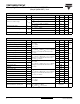
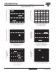
ELECTRICAL SPECIFICATIONS (T
J
= 25 °C unless otherwise specified)
PARAMETER SYMBOL TEST CONDITIONS MIN. TYP. MAX. UNITS
Collector to emitter breakdown voltage V
(BR)CES
V
GE
= 0 V, I
C
= 500 µA 600 - - V
Collector to emitter voltage V
CE(on)
V
GE
= 15 V, I
C
= 70 A - 2.1 2.4
V
V
GE
= 15 V, I
C
= 140 A - 2.8 3.4
V
GE
= 15 V, I
C
= 70 A, T
J
= 150 °C - 2.7 3
Gate threshold voltage V
GE(th)
I
C
= 0.5 mA 3 - 6
Collector to emitter leaking current I
CES
V
GE
= 0 V, I
C
= 600 V - - 0.7
mA
V
GE
= 0 V, I
C
= 600 V, T
J
= 150 °C - - 10
Gate to emitter leakage current I
GES
V
GE
= ± 20 V - - ± 250 nA
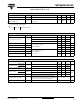
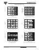
SWITCHING CHARACTERISTICS (T
J
= 25 °C unless otherwise specified)
PARAMETER SYMBOL TEST CONDITIONS MIN. TYP. MAX. UNITS
Total gate charge (turn-on) Q
g
I
C
= 70 A
V
CC
= 480 V
V
GE
= 15 V
- 460 690
nCGate to emitter charge (turn-on) Q
ge
- 160 250
Gate to collector charge (turn-on) Q
gc
-70130
Turn-on switching loss E
on
R
G
= 10 Ω
I
C
= 70 A, V
CC
= 480 V, V
GE
= 15 V, L = 200 µH
Energy losses include tail and diode reverse
recovery
-1.1-
mJ
Turn-off switching loss E
off
-0.9-
Total switching loss E
ts
-2-
Turn-on switching loss E
on
R
G
= 10 Ω
I
C
= 70 A, V
CC
= 480 V, V
GE
= 15 V, L = 200 µH
Energy losses include tail and diode reverse
recovery, T
J
= 150 °C
-1.27-
Turn-off switching loss E
off
-1.13-
Total switching loss E
ts
-2.4-
Turn-on delay time td
on
R
G
= 10 Ω
I
C
= 70 A, V
CC
= 480 V, V
GE
= 15 V, L = 200 µH
Energy losses include tail and diode reverse
recovery
- 314 -
ns
Rise time t
r
-49-
Turn-off delay time td
off
- 308 -
Fail time t
f
-68-
Turn-on delay time td
on
R
G
= 10 Ω
I
C
= 70 A, V
CC
= 480 V, V
GE
= 15 V, L = 200 µH
Energy losses include tail and diode reverse
recovery, T
J
= 150 °C
- 312 -
Rise time t
r
-50-
Turn-off delay time td
off
- 320 -
Fail time t
f
-78-
Input capacitance C
ies
V
GE
= 0 V
V
CC
= 30 V
f = 1.0 MHz
- 8000 -
pFOutput capacitane C
oes
- 790 -
Reverse transfer capacitance C
res
- 110 -
Reverse BIAS safe operating area RBSOA
T
J
= 150 °C, I
C
= 300 A
V
CC
= 400 V, V
P
= 600 V
R
G
= 22 Ω, V
GE
= + 15 V to 0 V
Fullsquare