6121 Baker Road, Suite 108 Minnetonka, MN 55345 Phone (952) 933-6190 Fax (952) 933-6223 1-800-274-4284 www.chtechnology.com Thank you for downloading this document from C&H Technology, Inc. Please contact the C&H Technology team for the following questions - Technical Application Assembly Availability Pricing Phone – 1-800-274-4284 E-Mail – sales@chtechnology.com www.chtechnology.com - SPECIALISTS IN POWER ELECTRONIC COMPONENTS AND ASSEMBLIES - www.chtechnology.
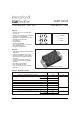
0MT120UF "FULL-BRIDGE" IGBT MTP UltraFast NPT IGBT Features • UltraFast Non Punch Through (NPT) Technology • Positive VCE(ON)Temperature Coefficient • 10µs Short Circuit Capability • HEXFRED TM Antiparallel Diodes with UltraSoft Reverse Recovery • Low Diode VF • Square RBSOA • Aluminum Nitride DBC • Very Low Stray Inductance Design for High Speed Operation • UL approved (File E78996) VCES = 1200V IC = 40A T C = 25°C Benefits • Optimized for Welding, UPS and SMPS Applications • Rugged with UltraFast P
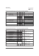
20MT120UF I27124 rev. D 02/03 Electrical Characteristics @ TJ = 25°C (unless otherwise specified) Parameters V(BR)CES ∆V(BR)CES/ ∆T J VCE(ON) Min Typ Max Units Test Conditions Collector-to-Emitter Breakdown Voltage 1200 Temperature Coeff. of Breakdown Voltage Collector-to-Emitter Saturation Voltage VGE(th) Gate Threshold Voltage ∆VGE(th) / Temperature Coeff. of ∆T J Threshold Voltage g fe I CES 3.29 4.42 3.87 5.32 3.99 4 3.59 4.66 4.11 5.70 4.
20MT120UF I27124 rev. D 02/03 Diode Characteristics @ TJ = 25°C (unless otherwise specified) Parameters Min V FM Diode Forward Voltage Drop Erec trr Irr Reverse Recovery Energy of the Diode Diode Reverse Recovery Time Peak Reverse Recovery Current Typ Max Units Test Conditions 2.48 3.28 2.44 3.45 2.21 420 98 33 2.94 3.90 2.84 4.14 2.
20MT120UF 50 250 40 200 30 150 Ptot (W) IC (A) I27124 rev. D 02/03 20 100 10 50 0 0 20 40 60 80 0 100 120 140 160 0 20 40 60 T C (°C) 80 100 120 140 160 TC (°C) Fig. 1 - Maximum DC Collector Current vs. Case Temperature Fig. 2 - Power Dissipation vs. Case Temperature 1000 1000 100 100 µs 1 1ms IC (A) IC (A) 100 10 µs 10 10 DC 0.1 1 0.01 1 10 100 1000 VCE (V) Fig.
20MT120UF I27124 rev. D 02/03 100 VGE VGE VGE VGE VGE = 15V = 12V = 10V = 8.0V VGE VGE VGE VGE VGE 80 60 ICE (A) ICE (A) 80 100 = 18V 40 20 = 18V = 15V = 12V = 10V = 8.0V 60 40 20 0 0 0 2 4 6 8 10 0 2 VCE (V) VGE VGE VGE VGE VGE 8 10 Fig. 6 - Typ. IGBT Output Characteristics TJ = 25°C; tp = 80µs 120 = 18V = 15V = 12V = 10V = 8.0V -40°C 25°C 125°C 100 80 60 IF (A) I CE (A) 80 6 V CE (V) Fig. 5 - Typ.
20MT120UF I27124 rev. D 02/03 20 20 18 16 ICE = 40A ICE = 20A 16 ICE = 10A ICE = 20A 14 ICE = 10A 14 ICE = 40A 12 VCE (V) VCE (V) 18 10 8 12 10 8 6 6 4 4 2 2 0 0 5 10 15 5 20 10 20 VGE (V) VGE (V) Fig. 10 - Typical VCE vs. VGE TJ = 25°C Fig. 9 - Typical VCE vs. VGE TJ = -40°C 20 300 18 16 ICE = 10A ICE = 20A 14 ICE = 40A T J = 25°C 250 T J = 150°C 200 12 ICE (A) VCE (V) 15 10 8 150 100 6 4 50 2 0 5 10 15 VGE (V) Fig. 11 - Typical VCE vs.
20MT120UF I27124 rev. D 02/03 2400 1000 2000 Energy (µJ) Swiching Time (ns) EON 1600 1200 EOFF 800 tdOFF tF 100 tdON 400 tR 0 10 0 10 20 30 40 0 50 10 20 IC (A) Fig. 13 - Typ. Energy Loss vs. IC TJ = 150°C; L=1.4mH; VCE= 400V RG= 5Ω; VGE= 15V 40 50 Fig. 14 - Typ. Switching Time vs. IC TJ = 150°C; L=1.
20MT120UF I27124 rev. D 02/03 40 40 RG = 5.0Ω 30 RG = 10 Ω IRR (A) IRR (A) 30 R G = 30 Ω 20 R G = 50 Ω 10 20 10 0 0 0 5 10 15 20 25 30 35 0 10 20 30 IF (A) 50 60 Fig. 18 - Typical Diode IRR vs. RG TJ = 150°C; IF = 5.0A Fig. 17 - Typical Diode IRR vs. IF TJ = 150°C 40 3.0 35 2.5 30 2.0 Q RR (µC) IRR (A) 40 RG ( Ω) 25 5.0Ω 10 Ω 20A 30Ω 1.5 50Ω 20 1.0 15 0.5 30A 10A 0.0 10 0 200 400 600 diF /dt (A/µs) Fig. 19- Typical Diode I RR vs.
20MT120UF I27124 rev. D 02/03 10000 Capacitance (pF) Cies 1000 Coes 100 Cres 10 0 20 40 60 80 100 VCE (V) Fig. 21- Typ. Capacitance vs. VCE VGE= 0V; f = 1MHz 16 14 600V 12 VGE (V) 10 8 6 4 2 0 0 40 80 120 160 200 Q G , Total Gate Charge (nC) Fig. 22 - Typical Gate Charge vs. VGE ICE = 5.0A; L = 600µH Document Number: 93588 www.vishay.
20MT120UF I27124 rev. D 02/03 1 Thermal Response ( Z thJC ) D = 0.50 0.20 0.1 0.10 0.05 0.02 0.01 0.01 τJ R1 R1 τJ τ1 R2 R2 τ2 τ1 R3 R3 τC τ τ2 τ3 τ3 Ci= τi/Ri Ci= i/Ri 0.001 Ri (°C/W) τi (sec) 0.161 0.000759 0.210 0.017991 0.147 0.06094 Notes: 1. Duty Factor D = t1/t2 2. Peak Tj = P dm x Zthjc + Tc SINGLE PULSE ( THERMAL RESPONSE ) 0.0001 1E-006 1E-005 0.0001 0.001 0.01 0.1 1 10 t1 , Rectangular Pulse Duration (sec) Fig 23.
20MT120UF I27124 rev. D 02/03 L L VCC DUT 0 80 V DUT 1000V Rg 1K Fig. CT.1 - Gate Charge Circuit (turn-off) Fig. CT.2 - RBSOA Circuit diode clamp / DUT L Driver D C 900V - 5V DUT / DRIVER DUT VCC Rg Fig. CT.3 - S.C. SOA Circuit Document Number: 93588 Fig. CT.4 - Switching Loss Circuit www.vishay.
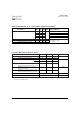
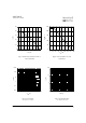
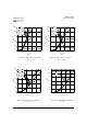
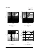
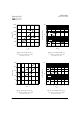
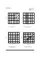
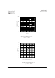
20MT120UF I27124 rev. D 02/03 Outline Table Electrical Diagram Resistance in ohms Dimensions in millimetres Document Number: 93588 www.vishay.
20MT120UF I27124 rev. D 02/03 Ordering Information Table Device Code 20 1 1 2 3 4 -5 6 MT 120 2 3 U F 4 5 Voltage Special Circuit Speed/ Current Essential Configuration Type Option rating code Part Number (20 (120 (U (F = 1200V) 20A) Ultra Full Bridge) Fast IGBT) Data and specifications subject to change without notice. This product has been designed and qualified for Industrial Level. Qualification Standards can be found on IR's Web site. IR WORLD HEADQUARTERS: 233 Kansas St.
Legal Disclaimer Notice Vishay Notice The products described herein were acquired by Vishay Intertechnology, Inc., as part of its acquisition of International Rectifier’s Power Control Systems (PCS) business, which closed in April 2007. Specifications of the products displayed herein are pending review by Vishay and are subject to the terms and conditions shown below. Specifications of the products displayed herein are subject to change without notice. Vishay Intertechnology, Inc.