
User Manual

www.vishay.com For technical questions, contact: indmodules@vishay.com
Document Number: 93223
2 Revision: 29-Apr-10
20MT060KF
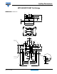
Vishay High Power Products
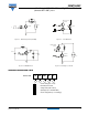
"Full Bridge" IGBT MTP
(Ultrafast NPT IGBT), 20 A
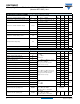
ELECTRICAL SPECIFICATIONS (T
J
= 25 °C unless otherwise noted)
PARAMETER SYMBOL TEST CONDITIONS MIN. TYP. MAX. UNITS
Collector to emitter breakdown voltage V
(BR)CES
V
GE
= 0 V, I
C
= 500 μA 600 - - V
Temperature coefficient of breakdown voltage ΔV
(BR)CES
/ΔT
J
V
GE
= 0 V, I
C
= 1 mA (25 to 125 °C) - + 0.6 - V/°C
Collector to emitter saturation voltage V
CE(on)
V
GE
= 15 V, I
C
= 20 A - 1.9 2.2
V
V
GE
= 15 V, I
C
= 40 A - 2.57 3.0
V
GE
= 15 V, I
C
= 20 A, T
J
= 125 °C - 2.22 2.5
V
GE
= 15 V, I
C
= 40 A, T
J
= 125 °C - 3.15 3.5
Gate threshold voltage V
GE(th)
V
CE
= V
GE
, I
C
= 250 μA 3.5 4.4 5.5
Temperature coefficient of threshold voltage V
GE(th)
/ΔT
J
V
CE
= V
GE
, I
C
= 1 mA (25 to 125 °C) - - 10 - mV/°C
Collector to emitter leaking current I
CES
V
GE
= 0 V, V
CE
= 600 V - 4 100
μA
V
GE
= 0 V, V
CE
= 600 V, T
J
= 125 °C - 80 200
Diode forward voltage drop V
FM
V
GE
= 0 V, I
F
= 20 A - 1.63 1.9
V
V
GE
= 0 V, I
F
= 40 A - 1.88 2.2
V
GE
= 0 V, I
F
= 20 A, T
J
= 125 °C - 1.32 1.6
V
GE
= 0 V, I
F
= 40 A, T
J
= 125 °C - 1.62 1.85
Gate to emitter leakage current I
GES
V
GE
= ± 20 V - - ± 200 nA
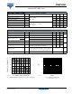
SWITCHING CHARACTERISTICS (T
J
= 25 °C unless otherwise specified)
PARAMETER SYMBOL TEST CONDITIONS MIN. TYP. MAX. UNITS
Total gate charge (turn-on) Q
g
I
C
= 20 A
V
CC
= 300 V
V
GE
= 15 V
-72-
nCGate to emitter charge (turn-on) Q
ge
-16-
Gate to collector charge (turn-on) Q
gc
-24-
Turn-on switching loss E
on
V
CC
= 360 V, I
C
= 20 A, V
GE
= 15 V,
R
g
= 5 Ω, L = 500 μH,
energy losses include tail and
diode reverse recovery
-0.18-
mJ
Turn-off switching loss E
off
-0.27-
Total switching loss E
tot
-0.45-
Turn-on switching loss E
on
V
CC
= 360 V, I
C
= 20 A, V
GE
= 15 V,
R
g
= 5 Ω, L = 500 μH, T
J
= 125 °C,
energy losses include tail and
diode reverse recovery
-0.25-
Turn-off switching loss E
off
-0.36-
Total switching loss E
tot
-0.61-
Turn-on delay time t
d(on)
-67-
ns
Rise time t
r
-23-
Turn-off delay time t
d(off)
- 101 -
Fall time t
f
- 127 -
Input capacitance C
ies
V
GE
= 0 V
V
CC
= 30 V
f = 1.0 MHz
- 1316 -
pFOutput capacitance C
oes
- 335 -
Reverse transfer capacitance C
res
-40-
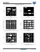
Reverse bias safe operating area RBSOA
T
J
= 150 °C, I
C
= 70 A
V
CC
= 400 V, V
p
= 600 V
R
g
= 22 Ω, V
GE
= + 15 V to 0 V
Fullsquare
Short circuit safe operating area SCSOA
T
J
= 150 °C
V
CC
= 400 V, V
p
= 600 V
R
g
= 22 Ω, V
GE
= + 15 V to 0 V
10 - - μs