
User Guide
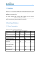
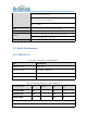
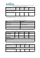

Table Of Contents

BroadLink
- 9 -
11
GPIO19
PWM7
SPI-MOSI
SD_D0
12
GPIO20
PWM0
SPI-MISO
SD_D1
13
VDD
14
GND
15
GPIO4
PWM4
16
GPIO1
PWM1
17
GPIO3
TX1
PWM2
I2C-SDA
SPI-SCL
18
GPIO2
RX1
PWM3
I2C-SCL
SPI-CS
Table 13 BL3372-P_1V1 pin definitions
Note:
1. In default, UART0 (pin4 and pin5) are used for bypass communication and UART2
(pin6 and pin7) are used for output of debugging information and burning firmware.
Please refer to the description in DC Characteristics for UART output current level.
2. RST is the reset pin and will be effective with VIL. Configuration information will be
remained after module reset. The module has pull-up process for RST designed
internally.
3. The pins for reset button and LED indication should be defined according to actual
firmware and circuit
4. GPIO0 and GPIO1 are hardware function pins and DO NOT pull up these two pins
before power-up.
5. Pulling up both GPIO0 and GPIO13 will switch the module to firmware programming
mode.
4.3 Recommendations
The following precautions should be considered during PCB designing:
Do not place any electrical components or grounding in antenna area on main board and
it’s better to leave this area blank on PCB.
It is recommended to not place any electrical components within 10mm range of module
antenna and not design any circuit or bond copper on main board under this area.
Do not use the module inside any metal case or containers with metal painting.
Keep the antenna of Wi-Fi module next to the edge of main board (as shown in Fig 5)
during design of PCB to ensure better performance of antenna.