
Datasheet


2
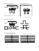
Block Layout
Figure 1. Block Layout of HSDL-9100
Pins Conguration Table
Notes:
Voltage to supply across the LED; VLED
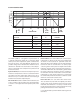
Absolute Maximum Ratings (Ta=25°C)
Electrical-Optical Characteristics (Ta=25°C)
Note:
1. I
Led
= 300mA Pulse, 5% Duty Cycle (Kodak 18% Reectance Gray Card)
LED
Photodiode
LED_A
LED_K
DET_K
DET_A
TOP VIEW
1
2
3
4
** L = 0 (zero light condition)
Pin Symbol Description Notes
1 LED_A LED Anode 1
2 LED_K LED Cathode -
3 DET_A Photodiode Anode -
4 DET_K Photodiode Cathode -
Parameter Symbol
Ratings
Units
Min. Max
Emitter
Continuous Forward Current I
DC
- 100 mA
Coupled
Total Power Dissipation (refer to Figure 1)
Operating Temperature
Storage Temperature
Reow Soldering Temperature
P
TOT
T
OP
T
STG
T
SOL
-
-40
-40
-
165
+85
+100
260
mW
°C
°C
°C
Parameter Symbol Test Condition
Ratings
UnitsMin Typ Max
Emitter
Forward Voltage
Reverse Voltage
Peak Wavelength
Spectrum Width of Half Value
V
F
V
R
l
p
D
p
I
F
= 100mA
I
R
= 10mA
I
F
= 20mA
I
F
= 20mA
-
5
-
-
1.50
-
940
50
1.65
-
-
-
V
V
nm
nm
Detector
Dark Current
Forward Voltage
Reverse Breakdown Voltage
I
Dark
V
F
V
BR
V
R
= 10V, L** = 0
I
F
= 10mA , L=0
I
R
= 100uA, L = 0
-
0.5
-
2
-
-
10
1.3
35
nA
V
V
Coupled
Output Current
Peak Output Distance
Operating Cross Talk Current
Rise Time (LED)
Fall Time (LED)
Rise Time (Photodiode)
Fall Time (Photodiode)
I
O
D
O
I
FD
T
RL
T
FL
T
RD
T
FD
Refer to Fig 2
Refer Note 1
Refer to Fig 3
R
L
= 50W
R
L
= 50W
R
L
= 5.1KW
R
L
= 5.1KW
-
-
-
-
-
-
-
10
5
-
50
50
6
6
-
-
200
-
-
-
-
mA
mm
nA
ns
ns
ms
ms