
Datasheet


14
Rg
1
3
V
SAT
2
4
8
6
7
5
+
V
CM
I
LEDP
C
LEDP
C
LEDN
SHIELD
* THE ARROWS INDICATE THE DIRECTION
OF CURRENT FLOW DURING ÐdV
CM
/dt.
+5 V
+
-
V
CC
= 18 V
***
***
0.1
µF
+
-
-
1
3
2
4
8
6
7
5
C
LEDP
C
LEDN
SHIELD
+5 V
Q1
I
LEDN
1
3
2
4
8
6
7
5
C
LEDP
C
LEDN
SHIELD
+5 V
Figure 21. Optocoupler input to output capacitance
model for unshielded optocouplers.
Figure 22. Optocoupler input to output capacitance
model for shielded optocouplers.
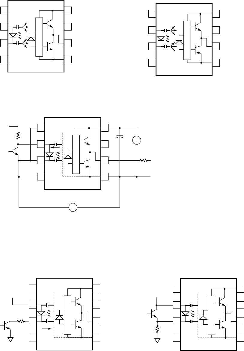
Figure 23. Equivalent circuit for Figure 17 during common mode transient.
Figure 24. Not recommended open collector drive circuit. Figure 25. Recommended LED drive circuit for ultra-high CMR
IPM dead time and propagation delay specications.
HCPL-J314 fig 22
1
3
2
4
8
6
7
5
C
LEDP
C
LEDN
1
3
2
4
8
6
7
5
C
LEDP
C
LEDN