
Datasheet


13
Selecting the Gate Resistor (Rg)
Step 1: Calculate R
g
minimum from the I
OL
peak speci-
cation. The IGBT and Rg in Figure 19 can be analyzed as
a simple RC circuit with a voltage supplied by the HCPL-
J314.
V
CC
– V
OL
Rg ≥ ————
I
OLPEAK
24 V – 5 V
= ————
0.6A
= 32 Ω
The V
OL
value of 5 V in the previous equation is the V
OL
at the peak current of 0.6A. (See Figure 6).
Step 2: Check the HCPL-J314 power dissipation and in-
crease Rg if necessary. The HCPL-J314 total power dissi-
pation (P
T
) is equal to the sum of the emitter power (P
E
)
and the output power (P
O
).
P
T
= P
E
+ P
O
P
E
= I
F
6 V
F
6 Duty Cycle
P
O
= P
O(BIAS)
+ P
O(SWITCHING)
= I
CC
6 V
CC
+ E
SW
(Rg,Qg) 6 f
= (I
CCBIAS
+ K
ICC
6 Qg 6 f) 6 V
CC
+ E
SW
(Rg,Qg) 6 f
where K
ICC
6 Qg 6 f is the increase in I
CC
due to switch-
ing and K
ICC
is a constant of 0.001 mA/(nC*kHz). For the
circuit in Figure 19 with I
F
(worst case) = 10 mA, Rg = 32
Ω, Max Duty Cycle = 80%, Qg = 100 nC, f = 20 kHz and
T
AMAX
= 85°C:
P
E
= 10 mA 6 1.8 V 6 0.8 = 14 mW
P
O
= (3 mA + (0.001 mA/(nC 6 kHz)) 6 20 kHz 6 100 nC) 6
24 V + 0.4 µJ 6 20 kHz = 80 mW
< 260 mW (P
O(MAX)
@ 85°C)
The value of 3 mA for I
CC
in the previous equation is the
max. I
CC
over entire operating temperature range.
Since P
O
for this case is less than P
O(MAX)
, Rg = 32 Ω is all
right for the power dissipation.
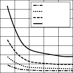
Figure 20. Energy dissipated in the HCPL-J314 and for
each IGBT switching cycle.
LED Drive Circuit Considerations for Ultra High CMR Perfor-
mance
Without a detector shield, the dominant cause of op-
tocoupler CMR failure is capacitive coupling from the
input side of the optocoupler, through the package, to
the detector IC as shown in Figure 21. The HCPL-J314
improves CMR performance by using a detector IC with
an optically transparent Faraday shield, which diverts the
capacitively coupled current away from the sensitive IC
circuitry. However, this shield does not eliminate the ca-
pacitive coupling between the LED and optocoupler pins
5-8 as shown in Figure 22. This capacitive coupling causes
perturbations in the LED current during common mode
transients and becomes the major source of CMR failures
for a shielded optocoupler. The main design objective of
a high CMR LED drive circuit becomes keeping the LED in
the proper state (on or o) during common mode tran-
sients. For example, the recommended application circuit
(Figure 19), can achieve 10 kV/µs CMR while minimizing
component complexity.
Techniques to keep the LED in the proper state are
discussed in the next two sections.
Esw – ENERGY PER SWITCHING CYCLE – µJ
0
0
Rg – GATE RESISTANCE – Ω
100
1.5
20
4.0
40
1.0
60 80
3.5
Qg = 50 nC
Qg = 100 nC
Qg = 200 nC
Qg = 400 nC
3.0
2.0
0.5
2.5