
Datasheet


12
Applications Information
Eliminating Negative IGBT Gate Drive
To keep the IGBT rmly o, the HCPL-J314 has a very low
maximum V
OL
specication of 1.0 V. Minimizing Rg and
the lead inductance from the HCPL-J314 to the IGBT gate
and emitter (possibly by mounting the HCPL-J314 on a
small PC board directly above the IGBT) can eliminate the
need for negative IGBT gate drive in many applications
as shown in Figure 19. Care should be taken with such a
PC board design to avoid routing the IGBT collector or
emitter traces close to the HCPL-J314 input as this can
result in unwanted coupling of transient signals into the
input of HCPL-J314 and degrade performance. (If the
IGBT drain must be routed near the HCPL-J314 input,
then the LED should be reverse biased when in the o
state, to prevent the transient signals coupled from the
IGBT drain from turning on the HCPL-J314.)
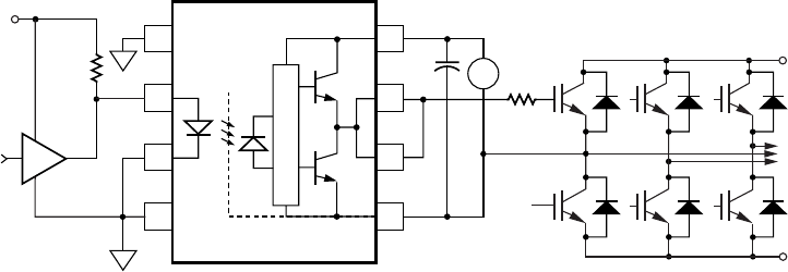
Figure 19. Recommended LED drive and application circuit for HCPL-J314.
+ HVDC
3-PHASE
AC
- HVDC
0.1 µF
V
CC
= 15 V
1
3
+
-
2
4
8
6
7
5
HCPL-J314
Rg
Q1
Q2
270 Ω
+5 V
CONTROL
INPUT
74XXX
OPEN
COLLECTOR